

Manufacturing method of a semiconductor device
a manufacturing method and semiconductor technology, applied in semiconductor devices, semiconductor/solid-state device details, electrical devices, etc., can solve the problem of not being able to effectively use the frame, and achieve the effect of compact semiconductor devices and preventing lead bending
- Summary
- Abstract
- Description
- Claims
- Application Information
AI Technical Summary
Benefits of technology
Problems solved by technology
Method used
Image

Examples
embodiment 1
[0184] (Embodiment 1)
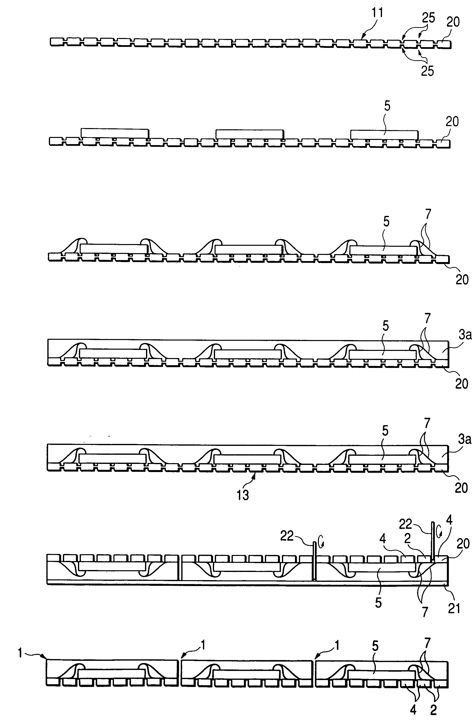
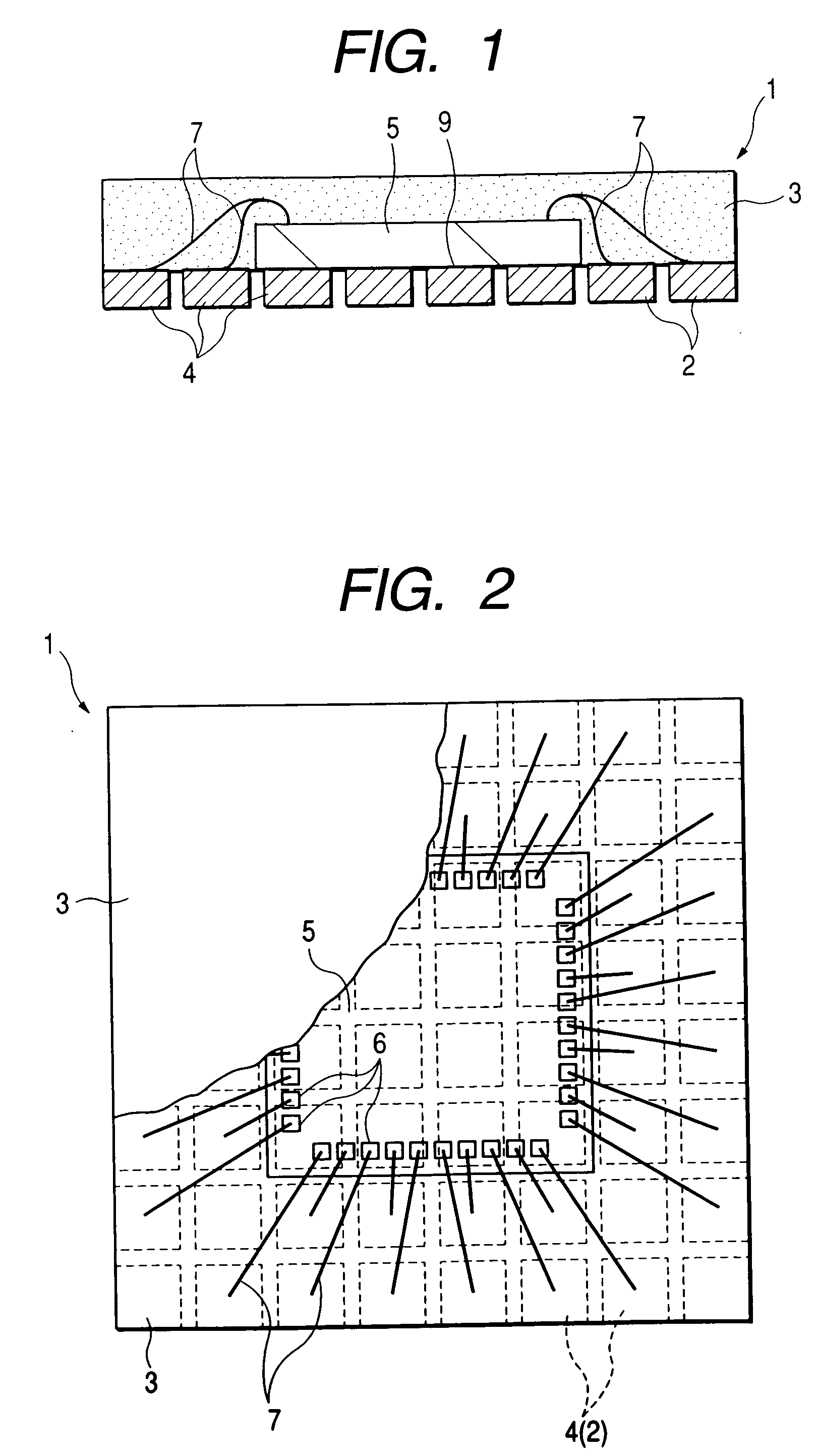
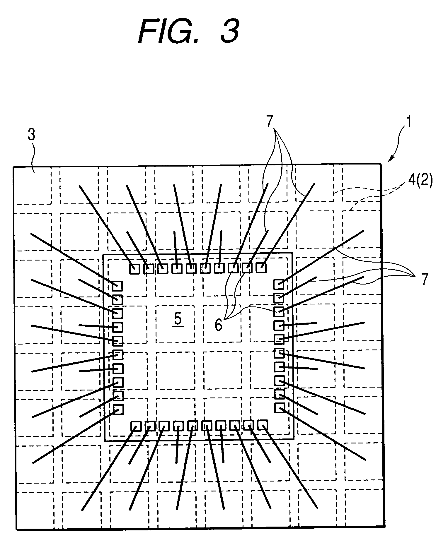
[0185]FIG. 1 to FIG. 13 are diagrams related to the method of manufacturing a non-leaded resin-sealed semiconductor device according to a first embodiment (Embodiment 1) of the invention. In Embodiment 1, in FIG. 1 to FIG. 4, an example is shown wherein the method of this invention is applied to the manufacture of a non-leaded semiconductor device 1 wherein external electrode terminals 2 comprising a conductive body (metal) are exposed on the rear surface of a square sealing package 33.
[0186] In Embodiment 1, as shown in FIG. 1 and FIG. 2, electrically isolated partition parts 4 (partition regions) 2 are provided in a grid pattern on the rear surface (mounting surface side) of a sealing package 3 comprising a rectangle of predetermined thickness. In Embodiment 1, a semiconductor device will be described wherein two rows of the partition parts 4 are provided as the external electrode terminals 2 along each side of the square resin sealing package.
[0187] The par...
embodiment 2
[0228] (Embodiment 2)
[0229]FIG. 14 and FIG. 15 are diagrams relating to the method of manufacturing the non-leaded semiconductor device according to another embodiment (Embodiment 2) of this invention. FIG. 14 is a cross-sectional view of the steps showing the method of manufacturing the semiconductor device, and FIG. 15 is a plan view of the substrate to which semiconductor elements are fixed and wires are attached.
[0230] In Embodiment 2, grooves25 are formed along the lines which cut the substrate 20 in Embodiment 1. The grooves 25 may be formed by a dicing blade or by etching, but are formed by etching in Embodiment 1. Regarding the forming of the grooves 25, although not shown, a photoresist film is provided over the whole surface of the substrate 20, and exposed to a predetermined pattern. Subsequently, the photoresist film is developed to form a checkered pattern of grooves, and the checkered pattern of grooves 25 is then provided on one surface of the substrate 20 by etching...
embodiment 3
[0253] (Embodiment 3)
[0254]FIGS. 16A to 16G are cross-sectional views of steps showing the method of manufacturing a non-leaded semiconductor device according to another embodiment (Embodiment 3) of this invention. In this Embodiment 3, the substrate 20 used in the manufacture of the semiconductor device 1 has a construction wherein, unlike Embodiment 2, the grooves 25 are provided in a checkered pattern on the side on which the semiconductor elements are fixed. In other words, the substrate 20 comprising the grooves 25 which was used in Embodiment 2 is inverted.
[0255] The method of manufacturing the non-leaded semiconductor device of Embodiment 3 will be described referring to the cross-sectional views of the steps of FIGS. 16A to 16G. As shown in FIG. 16A, after forming the checkered pattern of the grooves 25 on the upper surface (front surface), the semiconductor elements 5 are fixed to the surface where the grooves 25 are present as in Embodiment 1 and Embodiment 2.
[0256] Next...
PUM
 Abstract
Description
Claims
Application Information