Method for fabricating thin film pattern, device and fabricating method therefor, method for fabricating liquid crystal display, liquid crystal display, method for fabricating active matrix substrate, electro-optical apparatus, and electrical apparatus

a thin film pattern and active matrix technology, applied in static indicating devices, instruments, non-linear optics, etc., can solve the problem of liquid not readily spattering, and achieve the effect of increasing integration

Inactive Publication Date: 2005-01-06
SEIKO EPSON CORP
View PDF26 Cites 44 Cited by
  • Summary
  • Abstract
  • Description
  • Claims
  • Application Information

AI Technical Summary

Benefits of technology

[0072] According to the present invention, it becomes possible to carry out wiring formation in which the gate wiring, the source electrode, the drain electrode, and the pixel electrode do

Problems solved by technology

In addition, after building up the banks, when the function liquid is ejected (applied) to the concave part formed on the substrate between the banks, t

Method used


Image

  • Method for fabricating thin film pattern, device and fabricating method therefor, method for fabricating liquid crystal display, liquid crystal display, method for fabricating active matrix substrate, electro-optical apparatus, and electrical apparatus
  • Method for fabricating thin film pattern, device and fabricating method therefor, method for fabricating liquid crystal display, liquid crystal display, method for fabricating active matrix substrate, electro-optical apparatus, and electrical apparatus
  • Method for fabricating thin film pattern, device and fabricating method therefor, method for fabricating liquid crystal display, liquid crystal display, method for fabricating active matrix substrate, electro-optical apparatus, and electrical apparatus

Examples


first embodiment

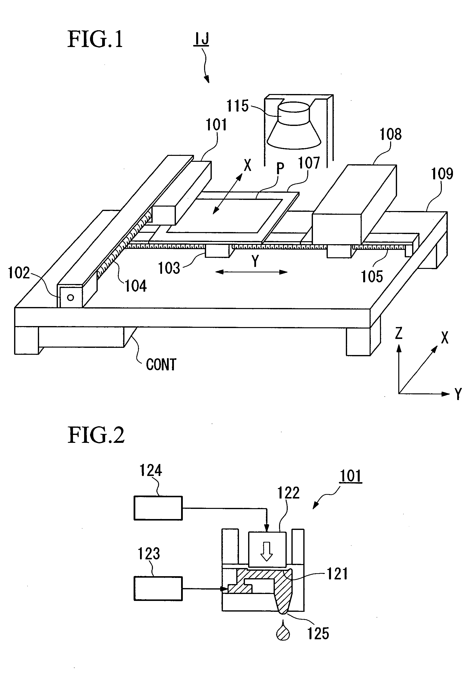
[0122] In the present embodiment, an example is explained for the case in which a wiring pattern (thin film pattern) ink (function liquid) that includes conductive particles is ejected as a droplet from the nozzle of a droplet ejection head using a droplet ejection method, and a wiring pattern formed by the conducting film is formed on the substrate.

[0123] The wiring pattern ink consists of a dispersant that disperses conductive particles into a dispersing medium, organic silver compounds, and a solvent that disperses silver oxide nanoparticles in a medium (dispersion medium).

[0124] In the present embodiment, in addition to using metal particles including any one among, for example, gold, silver, copper, palladium, and nickel as the conductive particles, the oxides thereof, along with conducting polymers and superconductive particles can be used.

[0125] These conductive particles can be used after the surface has been coated with organic substances in order to improve the dispersi...

second embodiment

[0187] Next, the fabricating method for the liquid crystal device of the present invention and the liquid crystal display fabricated by using this manufacturing method are explained below with reference to the figures. First, the fabricating method of the liquid crystal display of the present embodiment will be explained with reference to FIG. 5 to FIG. 14.

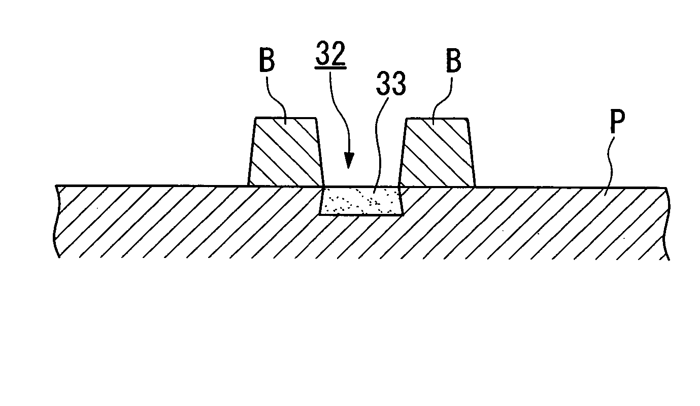
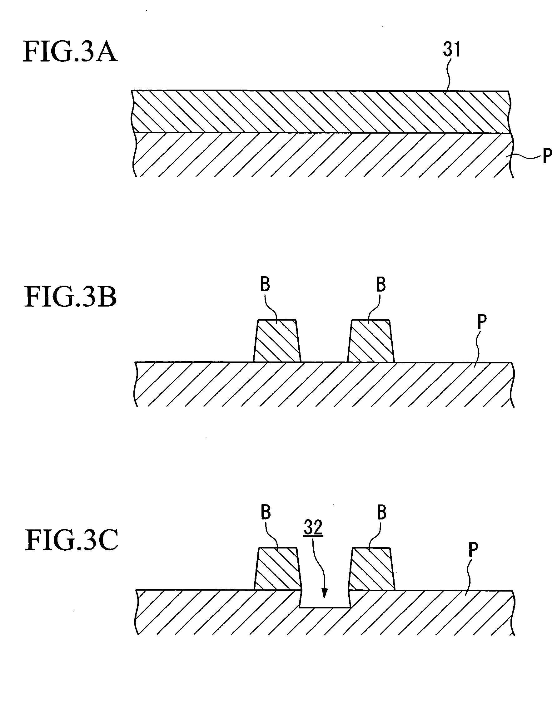
[0188] As shown in FIG. 5, in the substrate groove formation step, in the upper surface of a cleaned glass substrate 10, substrate grooves 10a having grove width of {fraction (1 / 20)} to {fraction (1 / 10)} that of the pitch of one pixel are applied by photoetching. Preferably, as shown in the figure, a forward-taper (a tapered profile that opens toward the ejection source) is used. Thereby, it becomes possible for the ejected droplet to fill the grooves down to the bottom.

[0189] Next, as shown in FIG. 6, in the liquid repelling part formation step, banks 11 are formed by lithography as a liquid repelling part that partitions the s...

third embodiment

[0213] Next, a fabricating method for a liquid crystal display of the present invention and the liquid crystal display fabricated by using this fabricating method will be explained below with reference to FIG. 15 to FIG. 22. Note that in these figures, essential elements identical to those in FIG. 5 through FIG. 14 shown in the second embodiment have identical reference numerals, and thus the explanation thereof is omitted.

[0214] As shown in FIG. 15, in the substrate groove formation step, in the upper surface of a cleaned glass substrate 10, substrate grooves 10a having grove width of {fraction (1 / 20)} to {fraction (1 / 10)} that of the pitch of one pixel are applied by photoetching. As shown in FIG. 19A and FIG. 19B, the substrate groove 10a is a groove in which the alternately traversing gate scanning line electrode 12, the capacity line 19c (explained below with reference to FIG. 22), the source electrode 15, and the drain electrode 19a (explained below with reference to FIG. 22)...


PUM


Abstract

A method for fabricating a thin film pattern on a substrate, includes the steps of: forming a concave part on the substrate that conforms to the thin film pattern; and applying a function liquid into the concave part.

Description

BACKGROUND OF THE INVENTION [0001] 1. Field of the Invention [0002] The present invention relates to a method for fabricating a thin film pattern, a device and fabricating method therefor, a method for fabricating a liquid crystal display, a liquid crystal display, a method for fabricating an active matrix substrate, an electro-optical apparatus, and an electrical apparatus. [0003] Priority is claimed on Japanese Patent Application No. 2003-155858, filed May, 2003, Japanese Patent Application No. 2003-155865, filed May, 2003, Japanese Patent Application No. 2003-155866, filed May, 2003, Japanese Patent Application No. 2003-155867, filed May, 2003, Japanese Patent Application No. 2004-103418, filed March, 2004, the contents of which are incorporated herein by reference. [0004] 2. Description of Related Art [0005] To fabricate a device having wiring used for electronic circuits or integrated circuits, a photolithographic method, for example, is used. This photolithographic method form...

Claims


Application Information

Patent Timeline
IPC IPC(8): B05D1/26G02F1/1343B05D5/12C30B1/00G02F1/133G02F1/1345G02F1/1362G02F1/1368H01L21/00H01L21/027H01L21/288H01L21/3205H01L21/336H01L21/768H01L21/77H01L21/84H01L27/12H01L27/32H01L29/786H01L51/40H01L51/56H05K3/00H05K3/10H05K3/12
CPCG02F1/13439G02F2001/136295H01L27/12H01L27/3211H01L51/0004H01L27/1292H05K3/1241H05K3/1258H05K2201/09036H05K2201/09909H05K3/107G02F1/136295H10K59/35H10K71/13G06K19/022A61L2/238
Inventor USHIYAMA, TOSHIHIROHIRAI, TOSHIMITSUMIKOSHIBA, TOSHIAKIKIGUCHI, HIROSHIHASEI, HIRONORI
Owner SEIKO EPSON CORP
Why Eureka
Try Eureka