

Method of inspecting pattern and inspecting instrument
a micro-miniature pattern and pattern technology, applied in the field of methods and instruments, to achieve the effect of high-quality inspection, easy setting of review conditions, and long tim
- Summary
- Abstract
- Description
- Claims
- Application Information
AI Technical Summary
Benefits of technology
Problems solved by technology
Method used
Image

Examples
Embodiment Construction
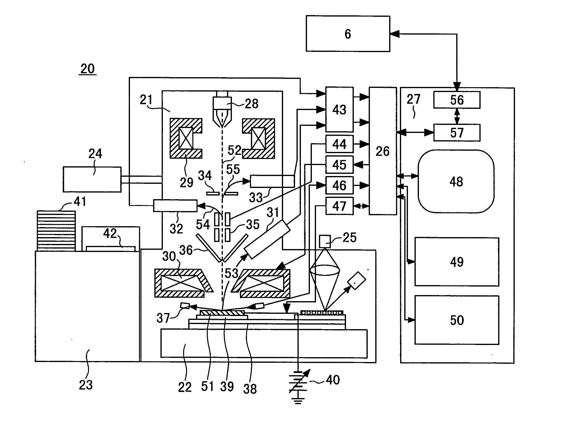
[0052] The pattern inspection system and the method of inspecting pattern of the present invention will be explained in detail with reference to the accompanying drawings.
[0053] In this embodiment, an inspection method and an inspection system will be explained to form an image using electron beam in order to detect existence of defect on a circuit pattern from such image and classify the contents of defect for the circuit pattern that is already inspected with the other inspection system. Here, as an example, inspection of a circuit pattern of a semiconductor device formed on a wafer will be explained.
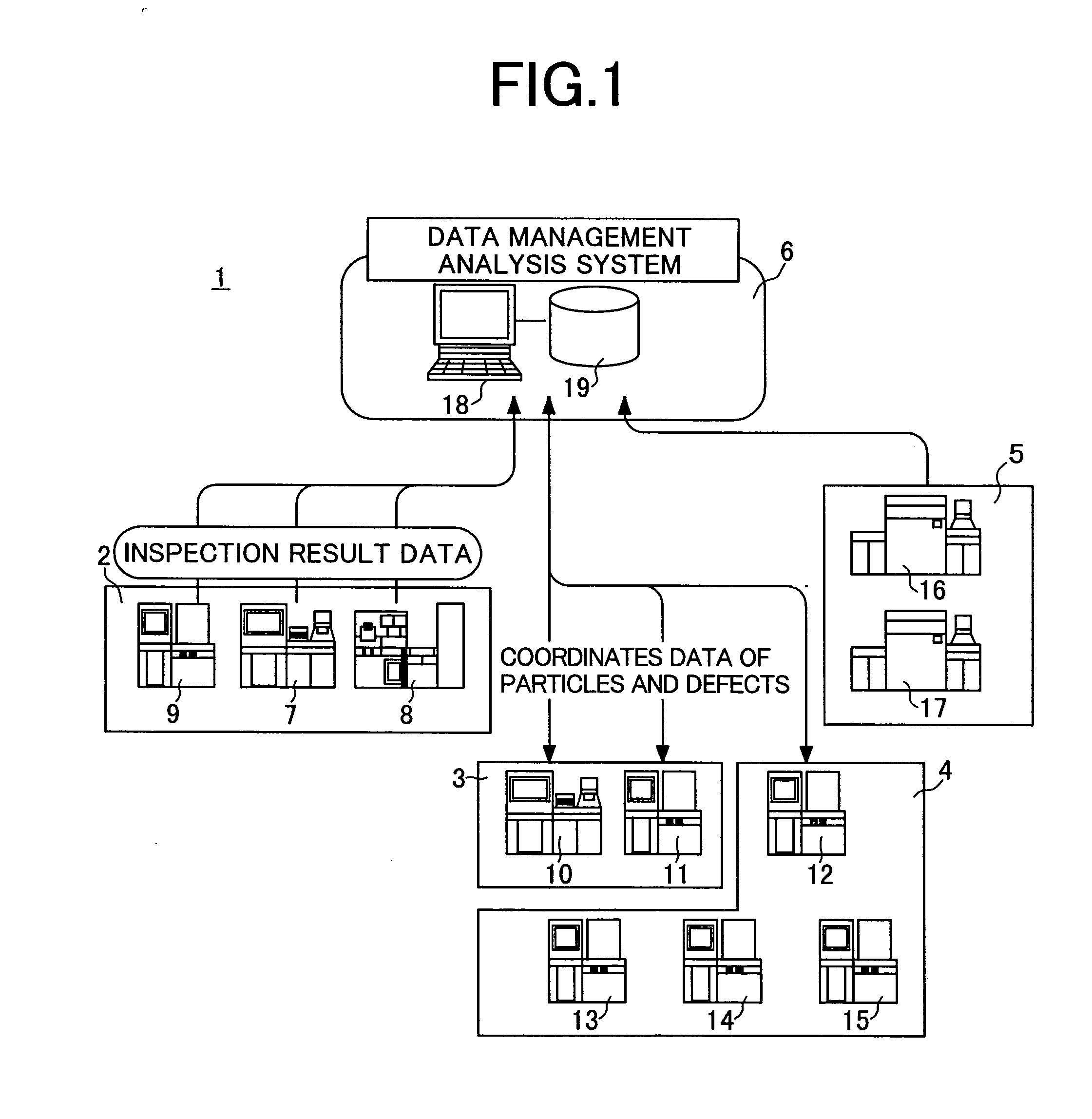
[0054] First, the outline of a pattern inspection system using a pattern inspection system of the present invention is illustrated in FIG. 1. The pattern inline inspection system 1 includes an inspection system 2 for finding out unknown particles and defects, a review system 3 for receiving an information of coordinates or the like of defect found out by the inspection system 2 to o...
PUM
| Property | Measurement | Unit |
|---|---|---|
| roughness | aaaaa | aaaaa |
| voltage contrast | aaaaa | aaaaa |
| defect inspecting | aaaaa | aaaaa |
Abstract
Description
Claims
Application Information