Semiconductor monolithic integrated optical transmitter

a monolithic, optical transmitter technology, applied in the direction of lasers, optical waveguide light guides, lasers, etc., can solve the problems of high power consumption of optical transmitters, high cost of optical transmitters, etc., and achieve the effect of minimizing light distortion and high power

Inactive Publication Date: 2005-01-13
SAMSUNG ELECTRONICS CO LTD
View PDF1 Cites 38 Cited by
  • Summary
  • Abstract
  • Description
  • Claims
  • Application Information

AI Technical Summary

Benefits of technology

[0010] Accordingly, the present invention has been made to reduce or overcome the above-mentioned limitations occurring in the prior art. One object of the present invention i

Problems solved by technology

However, in such a conventional optical transmitter 100, since each part is expensive, the entire cost of the optical transmitter 100 bec

Method used


Image

  • Semiconductor monolithic integrated optical transmitter
  • Semiconductor monolithic integrated optical transmitter
  • Semiconductor monolithic integrated optical transmitter

Examples


Embodiment Construction

[0022] Hereinafter, a preferred embodiment according to the present invention will be described with reference to the accompanying drawings. In the following description of the present invention, a detailed description of known functions and configurations incorporated herein will be omitted when it may make the subject matter of the present invention rather unclear.

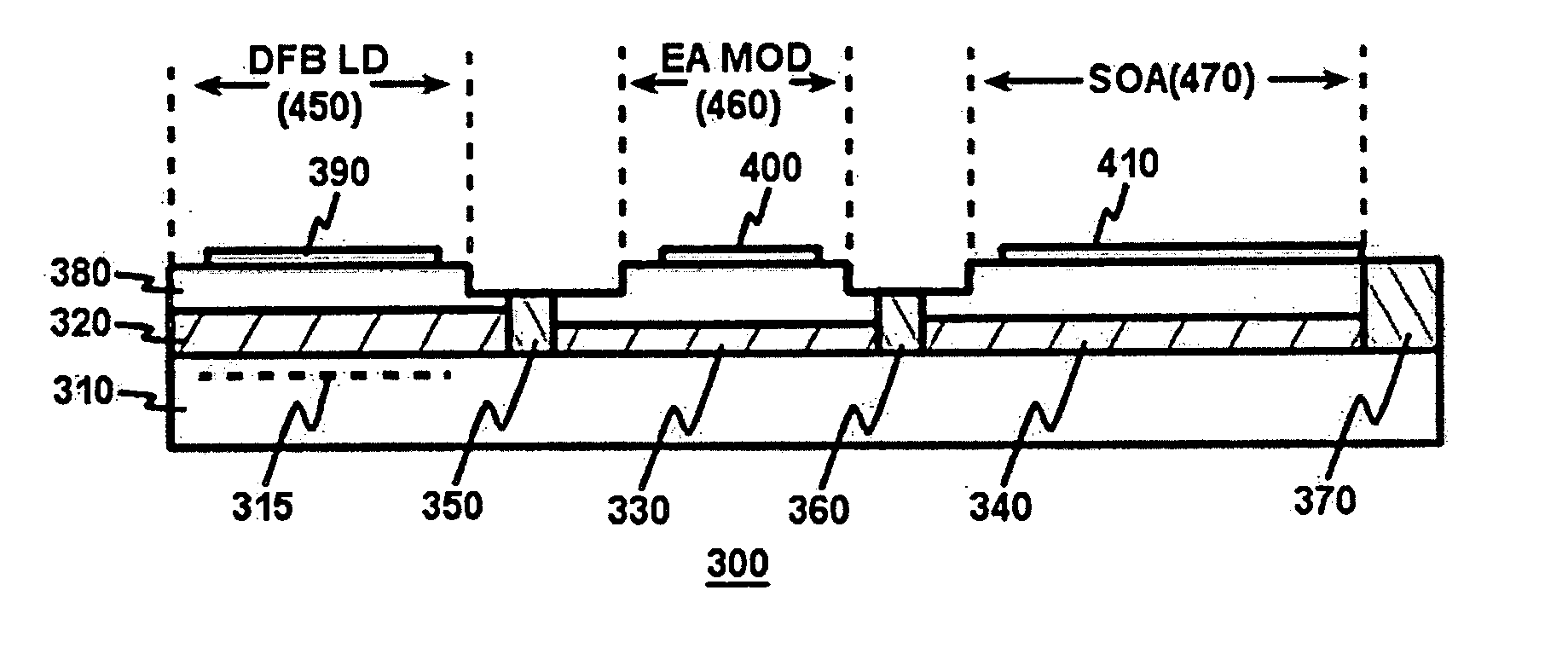
[0023]FIG. 3 is a perspective view of a monolithic integrated optical transmitter according to a preferred embodiment of the present invention. FIG. 4 is a cross-sectional view of the monolithic integrated optical transmitter shown in FIG. 3. The optical transmitter 300 has a monolithic integrated structure with a plurality of layers laminated on one semiconductor substrate 310. The plurality of layers includes a distributed feedback laser diode (hereinafter, referred to as DFB LD) 450 for oscillating light, an electro-absorption modulator (hereinafter, referred to as EA MOD) 460 for an optical intensity modulation, and...


PUM


Abstract

A semiconductor monolithic integrated optical transmitter including a plurality of active layers formed on a semiconductor substrate is disclosed, which comprises: a distributed feedback laser diode including a grating for reflecting light with a predetermined wavelength and a first active layer for oscillating received light from the grating; an electro-absorption modulator including a second active layer for receiving light from the first active layer, wherein the received light intensity is modulated through a change of absorbency in accordance with an applied voltage; an optical amplifier including a third active layer for amplifying received light from the second active layer; a first optical attenuator between the first active layer and the second active layer; and a second optical attenuator between the second active layer and the third active layer.

Description

CLAIM OF PRIORITY [0001] This application claims priority to an application entitled “Semiconductor monolithic integrated optical transmitter,” filed in the Korean Intellectual Property Office on Jul. 8, 2003 and assigned Serial No. 2003-46204, the contents of which are hereby incorporated by reference. BACKGROUND OF THE INVENTION [0002] 1. Field of the Invention [0003] The present invention relates to a semiconductor optical device, and more particularly to a semiconductor optical transmitter. [0004] 2. Description of the Related Art [0005] As Internet communication rapidly increases, the need for improved optical communication speed and facilities also increases. Further, rapid depreciation in optical part prices has promoted the construction of a new ultra-high speed communication environment. In such an environment, technologies are capable of realizing a modulation speed of more than 10 Gbps. In addition, long-distance transmission of more than 80 km without an erbium doped fib...

Claims


Application Information

Patent Timeline
IPC IPC(8): H01L33/00G02B6/12H01S5/026
CPCH01S5/0265H01S5/026G02B6/12
Inventor KANG, BYUNG-KWONCHO, SHI-YUNKIM, INRHEE, DO-YOUNGKIM, TAE-ILJANG, DONG-HOONLEE, SEUNG-WONJEON, DUK-HOAHN, JUNE-HYEONLEE, YOUNG-MINKIM, JONG-RYEOL
Owner SAMSUNG ELECTRONICS CO LTD
Why Eureka
Try Eureka