Semiconductor device and method for manufacturing the same

Inactive Publication Date: 2005-01-13
PANASONIC CORP
View PDF4 Cites 12 Cited by
  • Summary
  • Abstract
  • Description
  • Claims
  • Application Information

AI Technical Summary

Benefits of technology

[0050] When the third method for manufacturing a semiconductor device is used, compared with the example of FIG. 13 shown in “Background Art”, more rays in the ultraviolet region are incident on the active region serving as a diode when forming another insulating layer on the insulating layer obtained in the step (c) by a plasma process. Therefore, a

Problems solved by technology

This is because in the process for forming conductors of a semiconductor device, there is a limitation regarding the amount to be subjected to heat treatment because of diffusion of impurities, the heat resistance of a metal material for conductors and the like, and the amount to be subjected to heat treatment can be reduced by the plasma process.
However, with the increased utilization of the plasma process, device damage due to the plasma process tends to occur.
In a semiconductor device that is subjected to such plasma charging damage, the device characteristics are deteriorated, so that the semiconductor device is defective.
In the problem of plasma charging damage, in particular, deterioration in the reliability of gate insulating films constitutes a serious problem.
Therefore, the gate insulating film 26 is damaged and thus the device characteristics are damaged.
However, higher integration of the semiconductor device has been making the gate insulating film thinner year by year

Method used


Image

  • Semiconductor device and method for manufacturing the same
  • Semiconductor device and method for manufacturing the same
  • Semiconductor device and method for manufacturing the same

Examples


Example

[0075] Embodiment 1

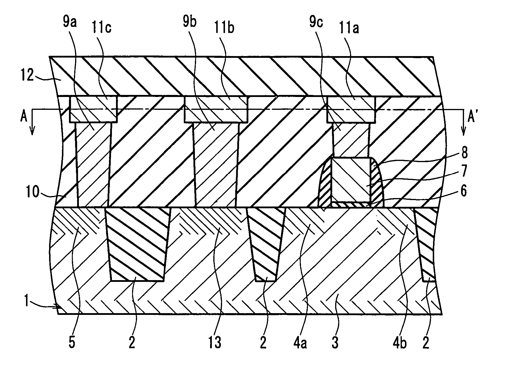
[0076] Hereinafter, a semiconductor device and a method for manufacturing the semiconductor device of Embodiment 1 of the present invention will be described with reference to FIGS. 1 and 2. First, the configuration of the semiconductor device of Embodiment 1 will be described with reference to FIG. 1.

[0077] As shown in FIG. 1A, the semiconductor device of Embodiment 1 includes an n-type silicon substrate 1 as in the semiconductor device shown in FIG. 11 described in “Background Art”, and a plurality of element separations 2 are formed on the silicon substrate 1 at a predetermined interval so as to be exposed on the silicon substrate 1.

[0078] Between the element separations 2 on the silicon substrate 1, an n-channel MOS transistor is formed with a p-well 3 formed in the internal portion of the n-type silicon substrate 1, a gate insulating film 6 and a gate electrode 7 formed of n+ polysilicon, and a source (n+) region 4a and a drain (n+) region 4b that are prov...

Example

[0096] Embodiment 2

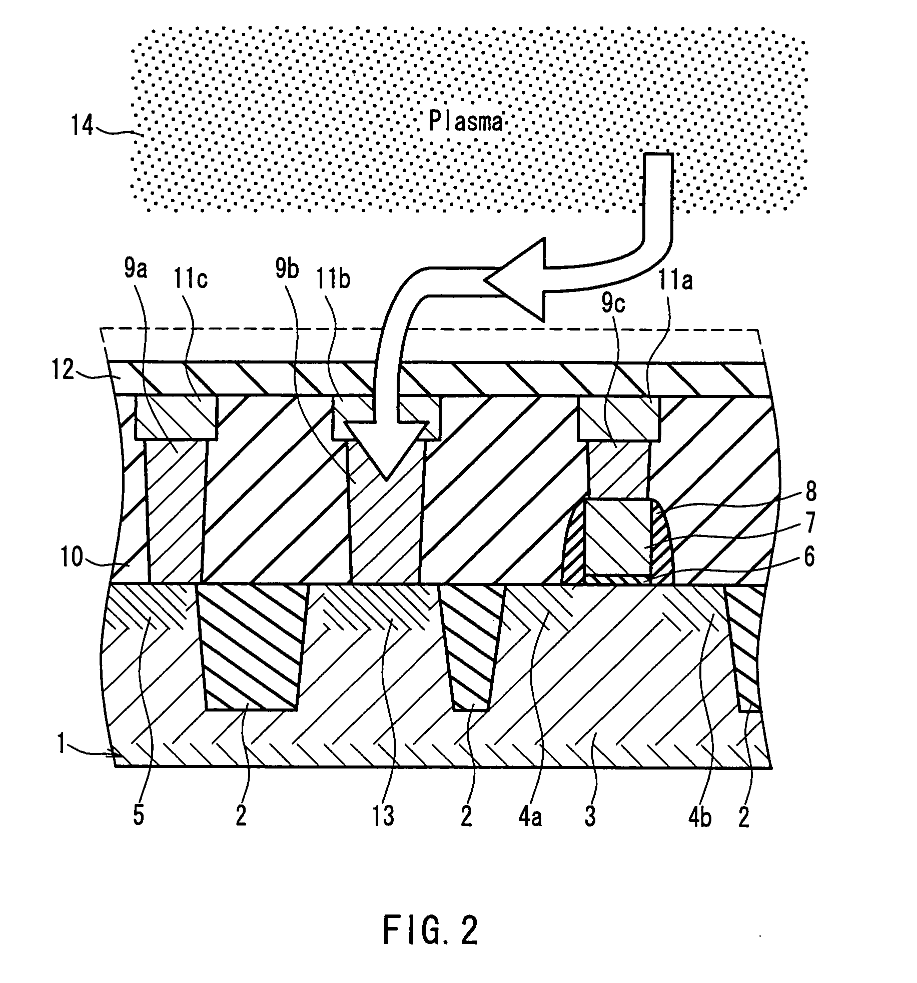
[0097] Next, a semiconductor device and a method for manufacturing the semiconductor device of Embodiment 2 of the present invention will be described with reference to FIGS. 3 and 4. First, the configuration of the semiconductor device of Embodiment 2 will be described with reference to FIG. 3. In FIGS. 3 and 4, the portion denoted by the same reference numeral as in FIG. 1 is the same portion as in FIG. 1.

[0098] As shown in FIG. 3, in Embodiment 2, unlike in Embodiment 1, a conductor 11d that is a second dummy conductor is provided. The conductor 11d also is formed simultaneously with the conductors 11a and 11b by the damascene method, but the entire circumference of the conductor 11d is insulated by the underlying interlayer insulating film 10 and the interlayer insulating film 12, and the conductor 11d is electrically suspended.

[0099] Next, a method for manufacturing the semiconductor device of Embodiment 2 and a function of dummy conductors will be describ...

Example

[0113] Embodiment 3

[0114] Next, a semiconductor device and a method for manufacturing the semiconductor device of Embodiment 3 of the present invention will be described with reference to FIGS. 6 to 9. First, the configuration of the semiconductor device of Embodiment 3 will be described with reference to FIG. 6.

[0115] As shown in FIG. 6A, the semiconductor device of Embodiment 3 includes a p-type silicon substrate 101 as in the semiconductor device shown in FIG. 13 described in “Background Art”, and a plurality of element separations 102 are formed on the silicon substrate 101 at a predetermined interval so as to be exposed on the silicon substrate 101.

[0116] Between the element separations 102 on the silicon substrate 101, a p-channel MOS transistor is formed with an n-well 103 formed in the internal portion of the silicon substrate 101, a gate insulating film 106 and a gate electrode 107 formed of p+ polysilicon, and a source (p+) region 104a and a drain (p+) region 104b that ...


PUM


Abstract

At least a laminate of a gate insulating film 6 and a gate electrode 7 and an active region 13 are formed on a silicon substrate 1, and an underlying interlayer insulating film 10 is further formed. Then, a conductor 11a connected to the gate electrode 7, and a conductor 11b that is a dummy conductor and is connected to the active region 13 are formed simultaneously on the underlying interlayer insulating film 10. Thereafter, an interlayer insulating film 12 is formed on the underlying interlayer insulating film 10 by a plasma process. At this time, charging current from a plasma 14 is emitted through the conductor 11b, which is a dummy conductor.

Description

TECHNICAL FIELD [0001] The present invention relates to a semiconductor device and a method for manufacturing the same. BACKGROUND ART [0002] In recent years, in a semiconductor device constituted by semiconductor integrated circuits, high integration has undergone great development. In particular, in semiconductor devices of MIS (metal insulated semiconductor) type, miniaturization and high performance of elements such as transistors have been promoted in order to cope with high integration, and there is a demand for further miniaturization and high performance. [0003] In a process for forming conductors of such a semiconductor device, plasma processing including plasma CVD or plasma etching has been increasingly utilized. This is because in the process for forming conductors of a semiconductor device, there is a limitation regarding the amount to be subjected to heat treatment because of diffusion of impurities, the heat resistance of a metal material for conductors and the like, ...

Claims


Application Information

Patent Timeline
IPC IPC(8): H01L21/768
CPCH01L21/76838
Inventor ERIGUCHI, KOJIMATSUMOTO, SUSUMU
Owner PANASONIC CORP
Why Eureka
Try Eureka