
Semiconductor integrated circuit device

a technology of integrated circuit devices and semiconductors, applied in the direction of semiconductor/solid-state device details, digital transmission, pulse automatic control, etc., can solve the problems of circuit diagram size and power dissipation, large error rate of latching data, and possible latching error, so as to reduce the error rate and prevent excessive following of input data jitters

Inactive Publication Date: 2005-01-13
HITACHI LTD
View PDF9 Cites 27 Cited by
  • Summary
  • Abstract
  • Description
  • Claims
  • Application Information

AI Technical Summary

Benefits of technology

[0020] It is an object of the present invention to provide a semiconductor integrated circuit device capable of reducing an error rate to a large extent of a bit synchronization circuit by preventing following excessively the jitters caused in input data.
[0021] Further, it is another object of the present invention to provide a semiconductor integrated circuit device capable of reducing the amount of changing phases of data and output clocks of the DLL circuit and the PLL circuit to a large extent by preventing following excessively the jitters contained in the data and reference clocks.

Problems solved by technology

However, the following problems are found by the inventor in data latching technique of the foregoing bit synchronization circuit:
Thus, a problem arises, in which data are acquired by a delay clock phase different from a clock phase for a period of the foregoing delay time, even if a data edge returns to an original position, and the error rate of latching data becomes large in the worst case since data cannot be read correctly.
Thus, the inventor noticed that a latching error might be caused in the worst case.
Thus, the inventor noticed that circuit diagram size and power dissipation became large.
Further, during phase matching using the majority decision circuit, if the number of majority decision counts of the majority decision circuit is small, then operation time from starting synchronization to actual synchronization becomes short, but the tolerance of the jitters becomes low.

Method used


Image

  • Semiconductor integrated circuit device
  • Semiconductor integrated circuit device
  • Semiconductor integrated circuit device

Examples


first embodiment

[0057] First Embodiment

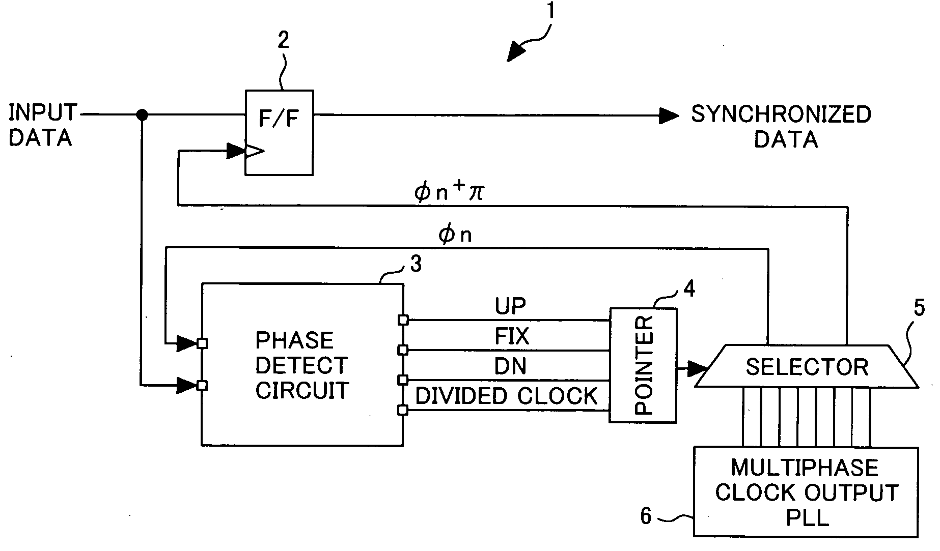
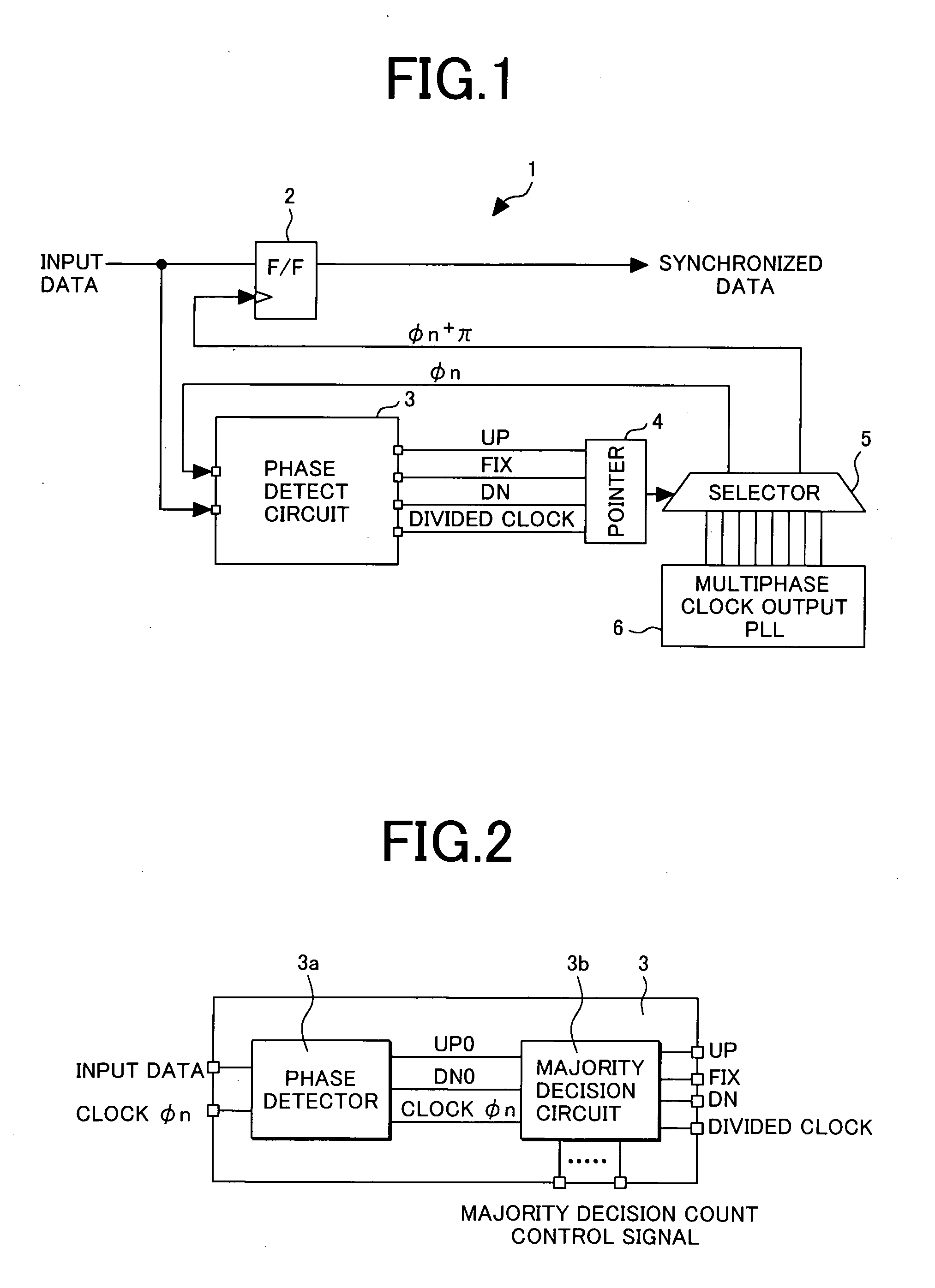
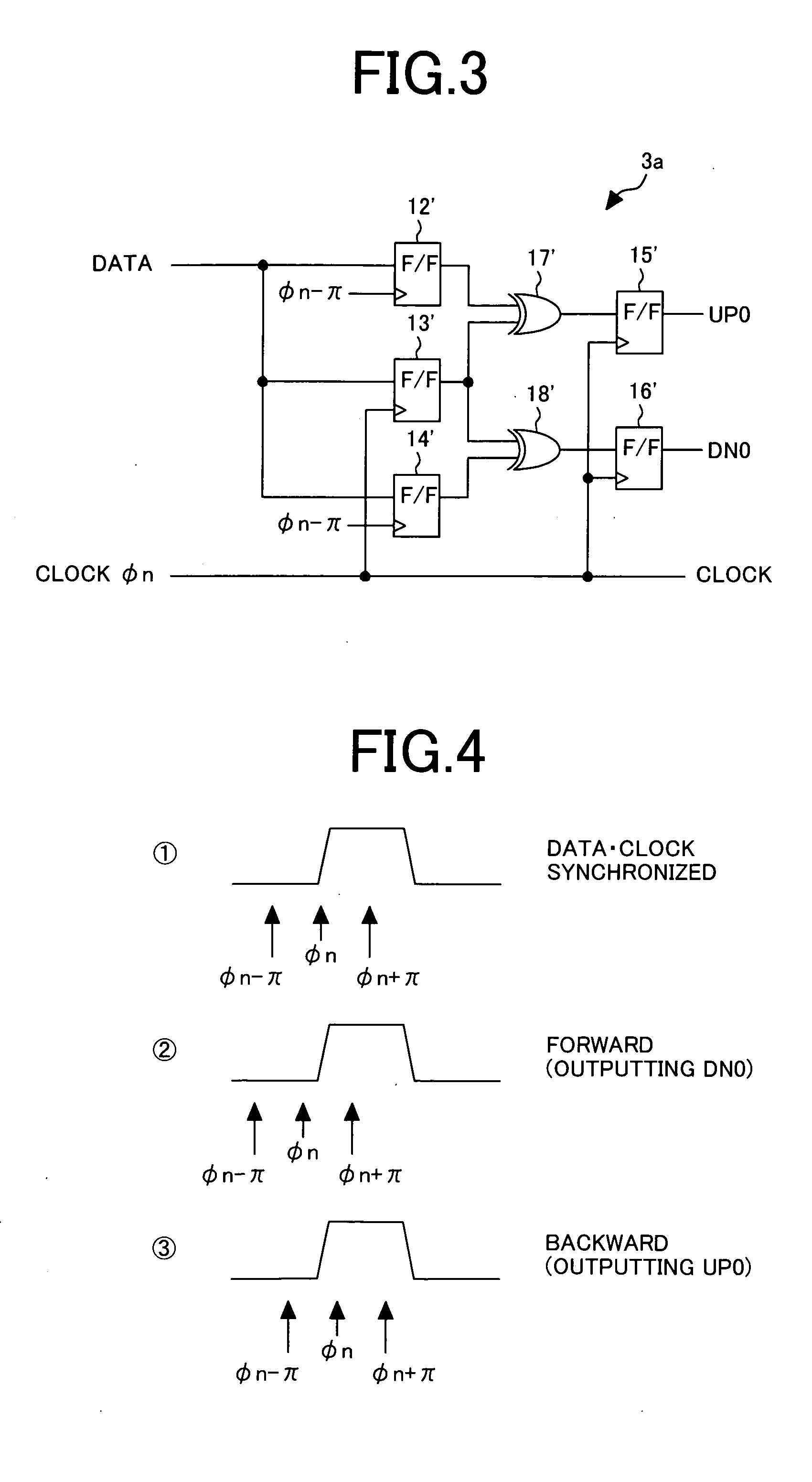
[0058]FIG. 1 is a block diagram of a bit synchronization circuit in the first embodiment of the present invention. FIG. 2 is a block diagram of a phase detect circuit using multiphase clocks provided in the bit synchronization circuit in FIG. 1. FIG. 3 is an example of a circuit diagram of a phase detect circuit using multiphase clocks. FIG. 4 shows a signal timing chart of the phase detect circuit in FIG. 3. FIG. 5 is another example of a circuit diagram of a phase detect circuit without using multiphase clocks. FIG. 6 shows a signal timing chart of each part of the phase detect circuit in FIG. 5. FIG. 7 is a circuit diagram of a majority decision circuit provided in the phase detect circuit in FIG. 2. FIG. 8 is a circuit diagram of a UP0 counter provided in the majority decision circuit in FIG. 7. FIG. 9 is a circuit diagram of a delay circuit provided in the majority decision circuit in FIG. 7. FIG. 10 is a circuit diagram of a magnitude relation determinat...

second embodiment

[0144] Second Embodiment

[0145]FIG. 20 is a block diagram of a phase detect circuit provided in a bit synchronous circuit in the second embodiment of the present invention. FIG. 21 is a circuit diagram of an example of a majority decision count control register provided in the phase detect circuit of FIG. 20. FIG. 22 is a block diagram of another example of the phase detect circuit of FIG. 20. FIG. 23 is a block diagram of another example of the phase detect circuit of FIG. 22.

[0146] In the second embodiment 2, the bit synchronous circuit includes the flip-flop 2, the phase detect circuit 31, the pointer 4, the selector 5, and the multiphase clock output PLL 6.

[0147] A phase detect circuit 31 includes the majority decision count control register 3c newly in addition to a circuit having the majority decision circuit 3b and the phase detector 3a in the same way as FIG. 5 of the foregoing embodiment.

[0148] The multiphase clock output PLL 6, the selector 5, the pointer 4, and the flip...


PUM


Abstract

An error rate of a bit synchronous circuit is decreased to a large extent by preventing following excessively the jitters included in input data. A phase detect circuit of a bit synchronous circuit includes a majority decision circuit. The majority decision circuit counts UP0 and DN0 signals as a phase comparison result of comparing phases by a UP0 counter and a DN0 counter for a period of time, and its count number is judged by a magnitude relation determination circuit. The magnitude relation determination circuit outputs an UP signal if the UP0 signal is majority, a DN signal if the DN0 signal is majority, and a FIX signal if the UP0 signal is equal to the DN0 signal. Accordingly, since it is possible to prevent following the jitters included in input data, etc., an error rate for bit synchronization can be reduced to a large extent.

Description

CLAIM OF PRIORITY [0001] The present invention claims priority from Japanese application JP 2003-194743 filed on Jul. 10, 2003, the content of which is hereby incorporated by reference into this application. FIELD OF THE INVENTION [0002] The present invention generally relates to phase control technique for data and clocks. More particularly, the present invention relates to effective application technique for reducing an error rate for a bit synchronization circuit. BACKGROUND OF THE INVENTION [0003] Conventionally, a bit synchronization circuit and the like, which correspond to various user's use conditions, are provided in a custom IC such as an application specific integrated circuit (ASIC). [0004] This bit synchronization circuit is a circuit for latching input data that are input asynchronously using a half cycle delayed clock from a data edge, which is output from a multiphase output phase locked loop (PLL) and synchronizing with clocks in a receiving side. [0005] Further, er...

Claims


Application Information

Patent Timeline
IPC IPC(8): H03L7/07H03L7/081H03L7/089H03L7/091H04L7/02H03L7/18H04L7/033
CPCH03L7/089H03L7/091H03L7/0814H04L7/0337H03L7/07H03L7/18
Inventor SUZUKI, KAZUHISA
Owner HITACHI LTD
Learn More