Atomic layer deposition of barrier materials

a barrier material and atomic layer technology, applied in the direction of coatings, chemical vapor deposition coatings, nanotechnology, etc., can solve the problems of increasing the overall resistance, and reducing the reliability of the overall circui

Inactive Publication Date: 2005-01-13
APPLIED MATERIALS INC
View PDF98 Cites 592 Cited by
  • Summary
  • Abstract
  • Description
  • Claims
  • Application Information

AI Technical Summary

Benefits of technology

[0009] A method is provided for depositing barrier layers on substrate surface using one or more atomic layer deposition techniques. In one aspect, a method is provided for processing a substrate including exposing the substrate to a soak process comprising a tungsten-containing compound and depositing a tantalum barrier layer on the substrate by an atomic layer deposition process, comprising exposing the substrate to sequential pulses of a tantalum precursor and a reductant.

Problems solved by technology

However, copper diffuses more readily into surrounding materials and can alter the electronic device characteristics of the adjacent layers and, for example, form a conductive path between layers, thereby reducing the reliability of the overall circuit and may even result in device failure.
Therefore, the additional amount of the barrier layer on the bottom of the feature not only increases the overall resistance of the feature, but also forms an obstruction between higher and lower metal interconnects of a multi-layered interconnect structure.

Method used


Image

  • Atomic layer deposition of barrier materials
  • Atomic layer deposition of barrier materials
  • Atomic layer deposition of barrier materials

Examples


examples

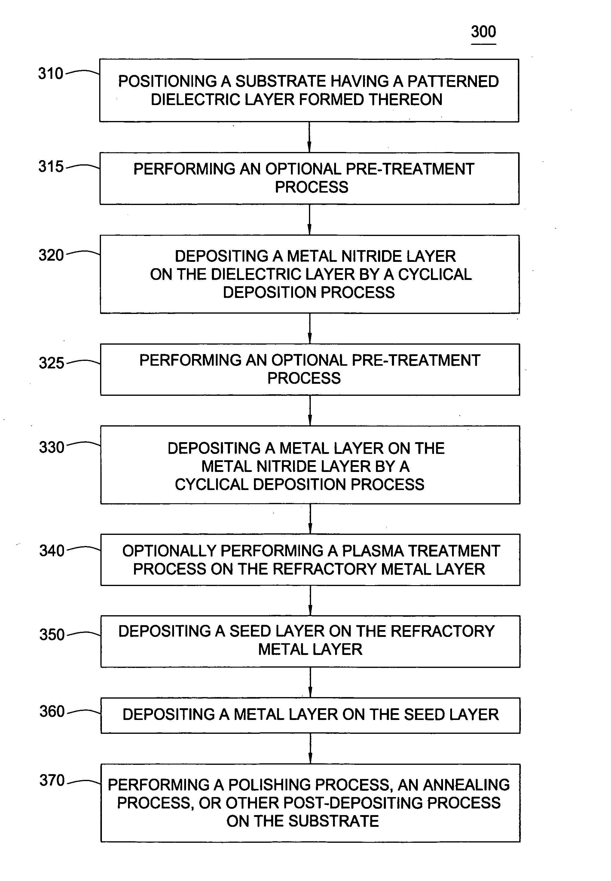
[0123] A tantalum (Ta) layer was deposited on a TaN layer by using a multi-step cyclical deposition process as follows with a soak process.

[0124] The tantalum nitride layer was formed by a process comprising flowing TaF5, SiH4 and NH3 or TaF5, NH3 and SiH4. For example, the tantalum nitride layer may be deposited at 325° C. by depositing about 5 Å TaN by a PDMAT / NH3 process, then a ten cycle process of NH3 for about 3 seconds, SiH4 for about 1 second, TaF5 for about 2 seconds, a SiH4 soak, and then a cycle of SiH4 for about 1 second and TaF5 for about 1 second.

[0125] The soak process forms an initial layer of tungsten by one or multiple cycles of diborane (B2H6) and tungsten fluoride (WF6) to prevent excessive silane (or disilane) exposures. The tungsten layer is exposed to small dose of siliane (or disilane) exposures to convert the surface to be SiH terminated such that the surface is ready to react with TaF5 to initiate ALD Ta growth. For example, the soak process may comprise ...


PUM

PropertyMeasurementUnit
diameteraaaaaaaaaa
diameteraaaaaaaaaa
aspect ratioaaaaaaaaaa

Abstract

Methods for processing substrate to deposit barrier layers of one or more material layers by atomic layer deposition are provided. In one aspect, a method is provided for processing a substrate including depositing a metal nitride barrier layer on at least a portion of a substrate surface by alternately introducing one or more pulses of a metal containing compound and one or more pulses of a nitrogen containing compound and depositing a metal barrier layer on at least a portion of the metal nitride barrier layer by alternately introducing one or more pulses of a metal containing compound and one or more pulses of a reductant. A soak process may be performed on the substrate surface before deposition of the metal nitride barrier layer and/or metal barrier layer.

Description

CROSS-REFERENCE TO RELATED APPLICATIONS [0001] This application claims benefit of U.S. Provisional Patent Application Ser. No. 60 / 479,426, filed Jun. 18, 2003, which is incorporated herein by reference.BACKGROUND OF THE INVENTION [0002] 1. Field of the Invention [0003] Embodiments of the present invention relate to a method for manufacturing integrated circuit devices. More particularly, embodiments of the invention relate to forming metal interconnect structures using one or more cyclical deposition processes. [0004] 2. Description of the Related Art [0005] As the structure size of integrated circuit (IC) devices is scaled down to sub-quarter micron dimensions, electrical resistance and current densities have become an area for concern and improvement. Multilevel interconnect technology provides the conductive paths throughout an IC device, and are formed in high aspect ratio features, including contacts, plugs, vias, lines, wires, and other features. A typical process for forming ...

Claims


Application Information

Patent Timeline
Patent Type & Authority Applications(United States)
IPC IPC(8): C23C16/02C23C16/14C23C16/44C23C16/455H01L21/28H01L21/285H01L21/44H01L21/4763H01L21/768
CPCC23C16/02C23C16/0281C23C16/14C23C16/45529H01L21/76876H01L21/76843H01L21/76862H01L21/76871H01L21/28562B82Y30/00C23C16/06
Inventor CHUNG, HUAWANG, RONGJUNMAITY, NIRMALYA
Owner APPLIED MATERIALS INC
Why Eureka
Try Eureka