Plasma processing material reclamation and reuse

a technology of material reclamation and plasma, applied in the field of material reclamation, can solve the problems of high material consumption, high cost of materials such as precursors, environmental and economic problems, etc., and achieve the effect of cost saving and less production of was

Inactive Publication Date: 2005-01-20
IBM CORP
View PDF10 Cites 3 Cited by
  • Summary
  • Abstract
  • Description
  • Claims
  • Application Information

AI Technical Summary

Benefits of technology

[0008] The invention includes an integrated circuit plasma processing system, apparatus and method for reclaiming material, such as a plasma precursor and potentially useful components among their byproducts, from plasma-enhanced exhaust of a plasma process chamber for subsequent reuse in the chamber. The apparatus provides a recycle feedback loop for a plasma process chamber that provides the high purity materials necessary for microelectronic applications. The apparatus is in-situ and does not introduce impurities into the reclaimed material. In addition to cost savings, the invention provides an environmentally friendly plasma process chamber and apparatus with very little production of waste.

Problems solved by technology

Manufacture of integrated circuits (ICs) by means of plasma-enhanced processing such as deposition and etch processes often involves the use of expensive precursors such as tungsten hexafluoride or tetra ethyl orthosilicate.
Exhausting such high percentages of material poses environmental issues and economic issues.
Unfortunately, either approach generally results in a significant waste stream of non-recovered material.
In terms of economics, materials such as a precursor are usually very expensive.
Accordingly, exhausting a high percentage of a precursor from plasma process chambers is very inefficient.
However, these approaches introduce impurities into the reclamation process, which destroys precursor purity and the ability to reuse the reclaimed precursor.

Method used


Image

  • Plasma processing material reclamation and reuse
  • Plasma processing material reclamation and reuse
  • Plasma processing material reclamation and reuse

Examples


Embodiment Construction

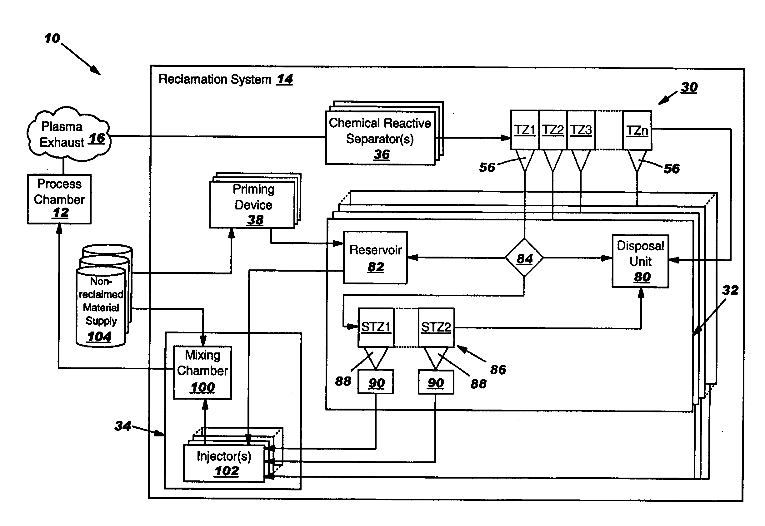
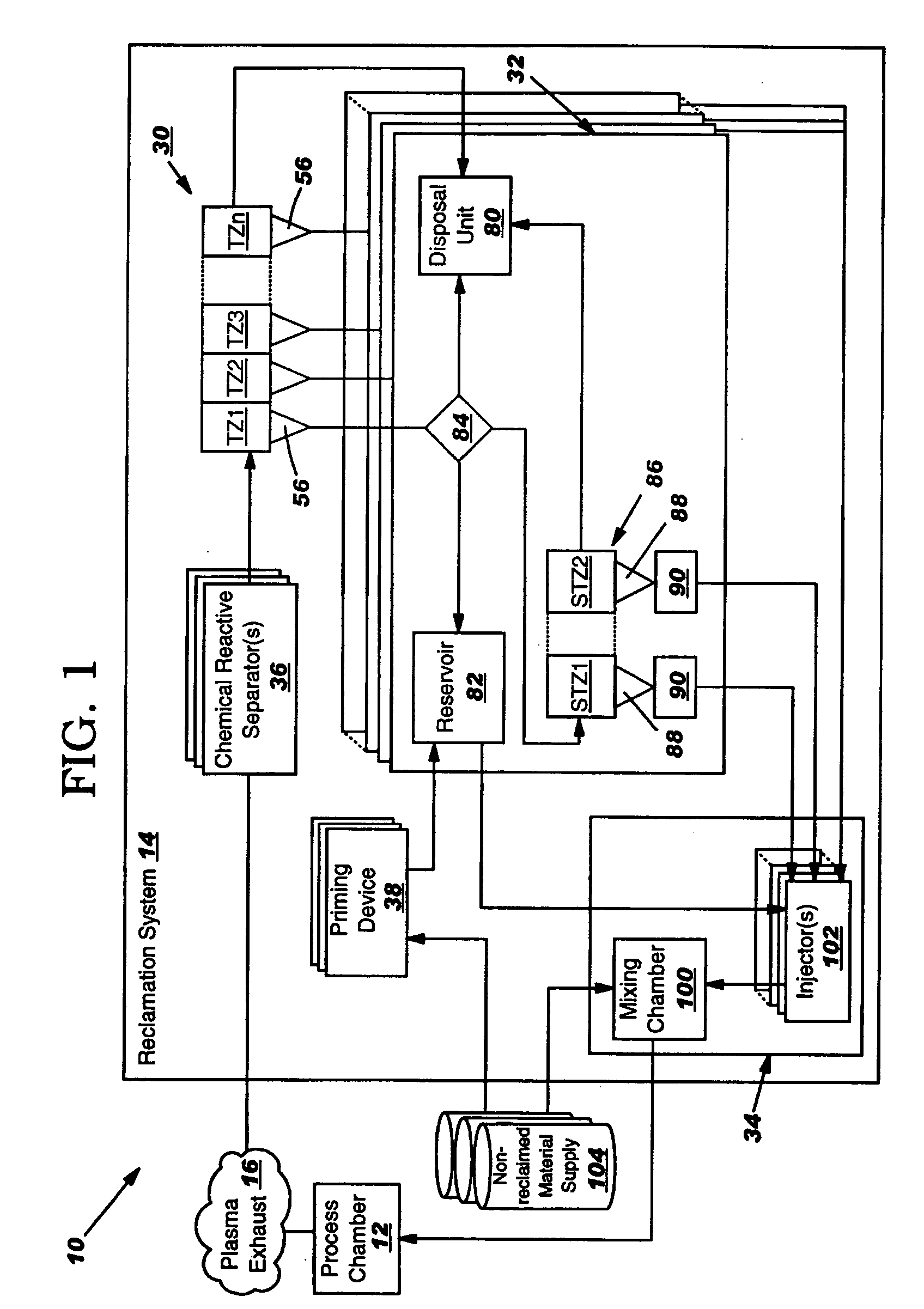
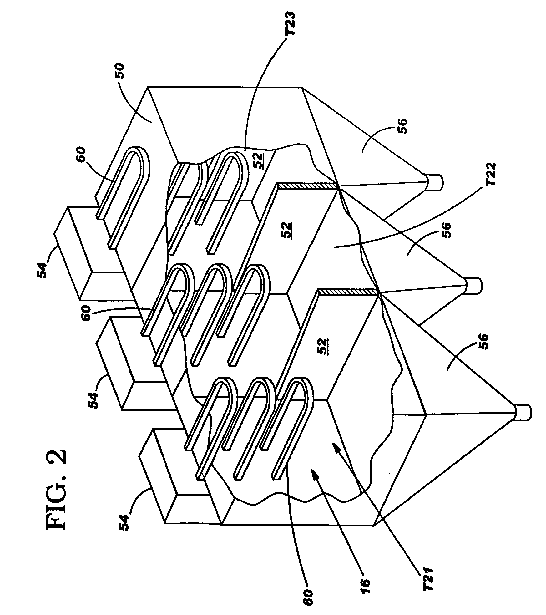
[0017] With reference to the accompanying drawings, FIG. 1 shows an integrated circuit (IC) plasma processing system 10 including a process chamber 12 and a reclamation (and reuse) system 14 according to the invention. Process chamber 12 may be any device for carrying out any now known or later developed plasma-enhanced processing. For example, plasma-enhanced chemical vapor deposition (PECVD) and / or reaction ion etching (RIE) on an IC wafer may be carried out in process chamber 12. Plasma-enhanced processing generally involves use of a carrier gas or diluent (e.g., a relatively inert gas such as nitrogen (N2)) in combination with appropriate reactants. For example, one plasma-enhanced process for deposition of silicon dioxide (SiO2) on a wafer can be accomplished by introduction of silane (SiH4) and nitrous oxide (N2O) into a nitrogen plasma at relatively low temperatures (i.e., 2) can be accomplished by introduction of tetra ethyl orthosilicate (TIOS) in an oxygen (O2) plasma.

[00...


PUM

PropertyMeasurementUnit
temperatureaaaaaaaaaa
heataaaaaaaaaa
purityaaaaaaaaaa

Abstract

An integrated circuit plasma processing system, apparatus and method for reclaiming material, such as a plasma precursor and potentially useful components among their byproducts, from plasma-enhanced exhaust of a plasma process chamber for subsequent reuse in the chamber. The apparatus provides a recycle feedback loop for a plasma process chamber that provides the high purity materials necessary for microelectronic applications. Since the apparatus is in-situ, no byproducts that are not already present are possible. Accordingly, the apparatus guarantees purity of the recycled material. In addition to cost savings, the invention provides an environmentally friendly plasma process chamber and apparatus with very little production of waste.

Description

BACKGROUND OF INVENTION [0001] 1. Technical Field [0002] The present invention relates generally to material reclamation, and more particularly, to plasma processing material reclamation and reuse. [0003] 2. Related Art [0004] Manufacture of integrated circuits (ICs) by means of plasma-enhanced processing such as deposition and etch processes often involves the use of expensive precursors such as tungsten hexafluoride or tetra ethyl orthosilicate. The percentage of precursor exhausted from plasma process chambers, either in original form or in the form of byproducts of plasma-induced reactions, can be very high. For example, for plasma-enhanced chemical vapor deposition (PECVD) of WF6 for tungsten deposition, approximately 82% of the tungsten is exhausted. Exhausting such high percentages of material poses environmental issues and economic issues. [0005] Relative to environmental issues, exhaust of such materials is generally to be avoided. Conventional approaches to addressing the ...

Claims


Application Information

Patent Timeline
Patent Type & Authority Applications(United States)
IPC IPC(8): C23C16/44C23C16/455H01J37/32
CPCC23C16/4412Y02C20/30H01J37/32844C23C16/45593
Inventor CHEN, BOMY A.FITZSIMMONS, JOHN A.MCGAHAY, VINCENT J.RYAN, JAMES G.SMETANA, PAVEL
Owner IBM CORP
Why Eureka
Try Eureka