Semiconductor device

Inactive Publication Date: 2005-01-20
RENESAS ELECTRONICS CORP
View PDF12 Cites 20 Cited by
  • Summary
  • Abstract
  • Description
  • Claims
  • Application Information

AI Technical Summary

Benefits of technology

[0013] In a semiconductor device having a spiral inductor, an object of the present invention is to pr

Problems solved by technology

However, various problems exist due to substrate floating effect, e.g. carries (holes in NMOS) produced by impact ionization accumulate in the channel formation region to cause kinks or deteriorate the operating breakdown voltage, and the unstable potential of the channel formation region causes frequency dependency of delay time.
However, in an SOI device adopting the PTI structure and having a spiral inductor (an inductance element), if the PTI structure is present under the inductor, the current flowing in the spiral inductor causes eddy current in the SOI layer (silicon layer) between the trench bottom and

Method used


Image

  • Semiconductor device
  • Semiconductor device
  • Semiconductor device

Examples


Embodiment Construction

[0022]

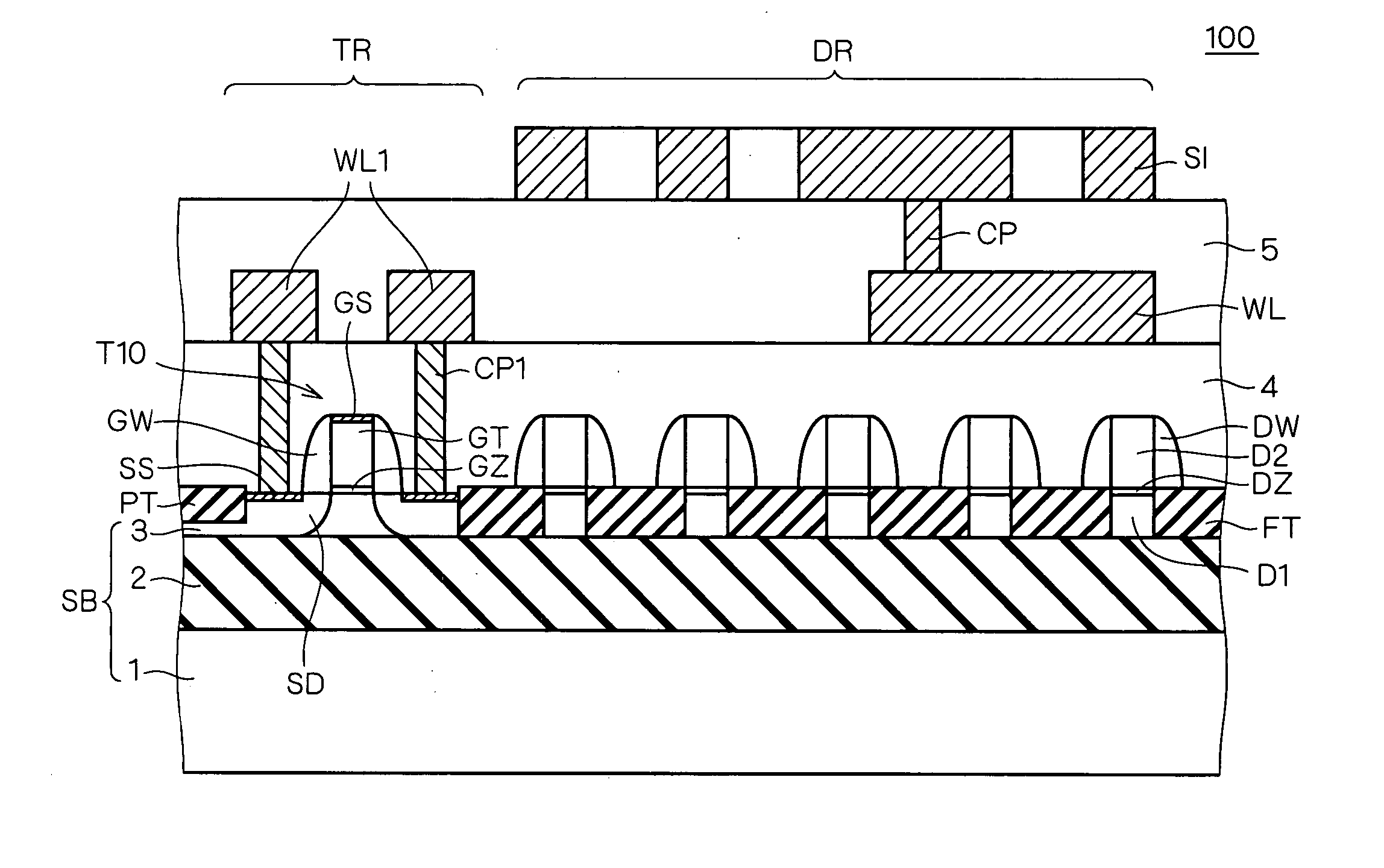
[0023] First, an example of the structure of a spiral inductor is described referring to FIG. 1. As shown in FIG. 1, a spiral inductor SI is formed by spirally winding an interconnection, whose one end at the center of the spiral is connected to a lower-layer interconnection WL through a contact CP passing through an interlayer insulating film (not shown). The other end of the spiral inductor SI is connected to an interconnection lying in the same layer as the spiral inductor SI, which is not shown in the drawing. The description below is made assuming that the spiral inductor SI is thus constructed.

[0024]

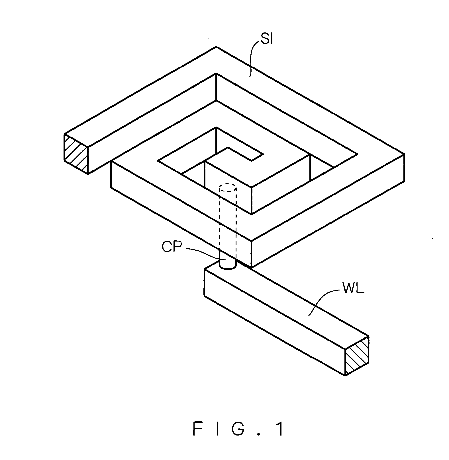
[0025] Next, the structure of a semiconductor device 100 according to the preferred embodiment of the invention is described referring to FIG. 2.

[0026] In FIG. 2, an SOI substrate SB is formed of a silicon substrate 1, a buried oxide film 2 provided on the silicon substrate 1, and an SOI layer 3 provided on the buried oxide film 2. The SOI substrate SB is sectioned into a t...


PUM


Abstract

A transistor region is a region where a plurality of MOS transistors, including an MOS transistor, are formed, and a dummy region is a region lying under a spiral inductor. In the dummy region, a plurality of dummy active layers are disposed in the main surface of an SOI substrate and a plurality of dummy gate electrodes are disposed covering the respective dummy active layers. The arrangement pattern of the dummy active layers and the arrangement pattern of the dummy gate electrodes nearly match, so that the dummy gate electrodes are aligned accurately on the dummy active layers.

Description

BACKGROUND OF THE INVENTION [0001] 1. Field of the Invention [0002] The present invention relates to semiconductor devices and particularly to a semiconductor device having an inductor. [0003] 2. Description of the Background Art [0004] SOI (Silicon On Insulator) structure semiconductor devices (hereinafter referred to as SOI devices), which are formed on an SOI substrate having a silicon substrate and a buried oxide film and an SOI layer lying on the silicon substrate, offer reduced parasitic capacitance, stable high-speed operation, and reduced power consumption. The SOI devices are used in portable devices, for example. [0005] Examples of the SOI devices include full trench isolation (FTI) structure SOI devices, in which elements are electrically isolated from each other by a full trench isolation insulating film formed by burying an insulator in a trench that is formed in the surface of the SOI layer to reach the buried oxide film. However, various problems exist due to substrat...

Claims


Application Information

Patent Timeline
IPC IPC(8): H01L21/76H01L21/822H01L21/762H01L21/8234H01L21/84H01L23/522H01L27/01H01L27/04H01L27/06H01L27/08H01L27/088H01L27/12H01L29/786
CPCH01L21/84H01L23/5227H01L27/1203H01L2924/0002H01L2924/00H01L27/04
Inventor IPPOSHI, TAKASHI
Owner RENESAS ELECTRONICS CORP
Why Eureka
Try Eureka