Etching method and plasma etching processing apparatus

a plasma etching and processing method technology, applied in the direction of electrical equipment, basic electric elements, electric discharge tubes, etc., can solve the problems of not disclosing the method for forming holes (or grooves), difficult to form deep holes in silicon, etc., to achieve the effect of more accurate control of the shape of the holes or grooves being formed and the flow ra

Inactive Publication Date: 2005-01-20
TOKYO ELECTRON LTD +1
View PDF4 Cites 24 Cited by
  • Summary
  • Abstract
  • Description
  • Claims
  • Application Information

AI Technical Summary

Benefits of technology

[0014] The second step may be executed by increasing the second high-frequency power compared to the first step. In addition, the second step may include a plurality of steps. When executing the individual steps constituting the second step, the level of the second high-frequency power and the flow rate of the O2 gas may be varied. It is particularly desirable to set a higher flow rate for the O2 gas in later steps among the plurality of steps constituting the second step. Through this method, the shape of the holes or grooves being formed can be controlled more accurately.

Problems solved by technology

However, a satisfactory etching selection ratio, which is a ratio of the etching rate of silicon, i.e., the target material being etched, to the etching rate of a silicon oxide film used as a mask during the etching process (hereafter simply referred to as an etching selection ratio) is not achieved with the first method described above, and for this reason, it is difficult to form deep holes in the silicon while ensuring that the mask remains unetched over the required thickness.
However, it does not disclose a method for forming holes (or grooves) having a very small hole diameter (or a groove with) of 1 μm or smaller (e.g., approximately 0.2 μm).

Method used


Image

  • Etching method and plasma etching processing apparatus
  • Etching method and plasma etching processing apparatus
  • Etching method and plasma etching processing apparatus

Examples


first embodiment

[0046] (First Embodiment)

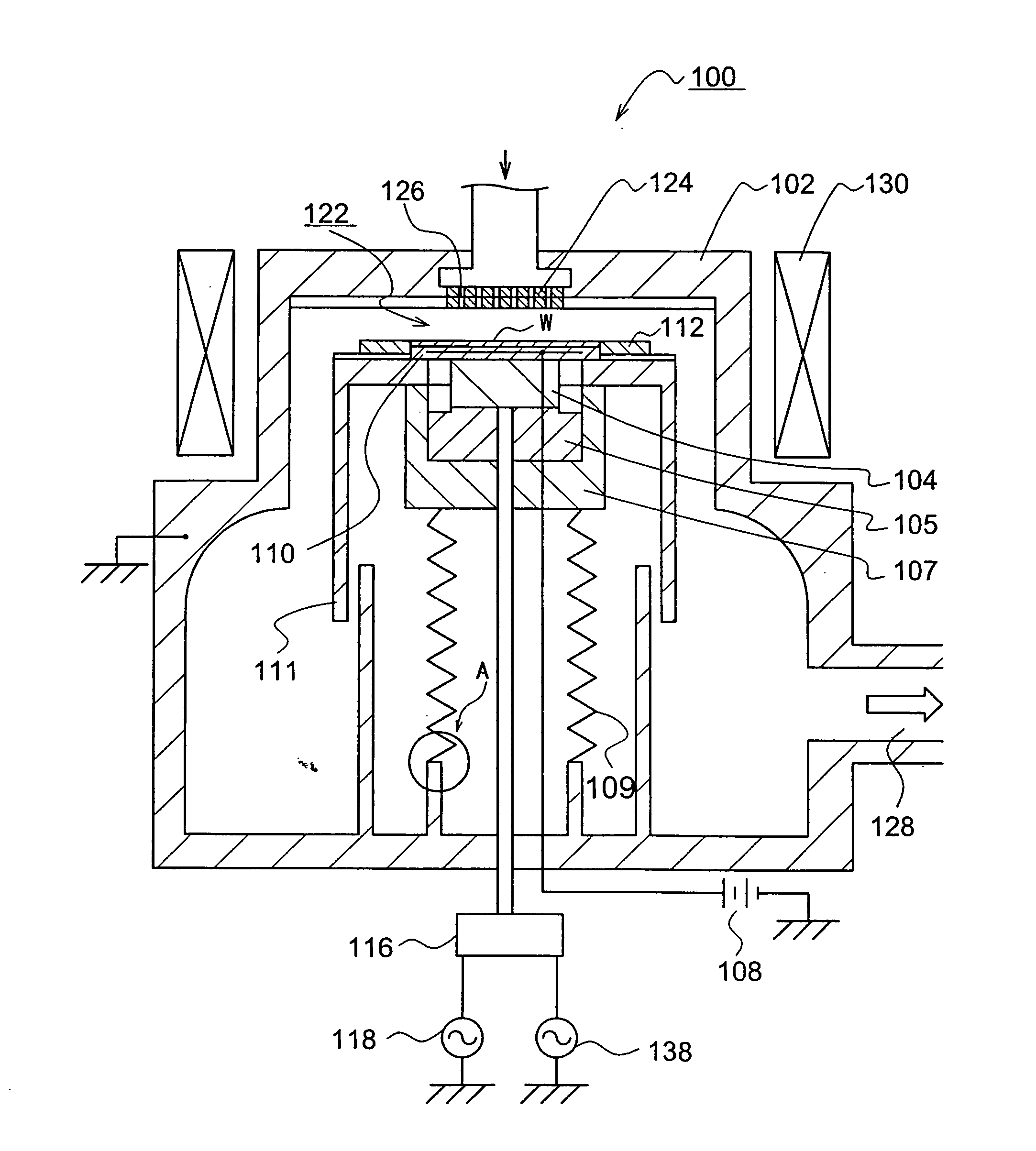
[0047]FIG. 1 is a schematic sectional view of the structure of a plasma etching apparatus 100 achieved in an embodiment of the present invention. A processing container 102 of the plasma etching apparatus 100 in FIG. 1 is constituted of aluminum having an aluminum oxide film formed at the surface thereof through, for instance, anodizing and is grounded.

[0048] A lower electrode 104 to be used as a stage on which a workpiece such as a semiconductor wafer W is placed and also to function as a susceptor is disposed within the processing container 102. The lower electrode 104 is allowed to move up / down freely by an elevator shaft (not shown).

[0049] Over the lower area of the side surface of the lower electrode 104, a quartz member 105 to function as an insulating member and a conductive member 107 which is placed in contact with a bellows 109 are formed. The bellows 109, which may be constituted of, for instance, stainless steel, is in contact with the processi...


PUM


Abstract

When etching a silicon layer 210 with a processing gas containing a mixed gas constituted of HBr gas, and O2 gas and SiF4 gas and further mixed with both of or either of SF6 gas and NF3 gas by using a pre-patterned mask having a silicon oxide film layer 204 inside an airtight processing container 102, high-frequency power with a first frequency is applied from a first high-frequency source 118 and high-frequency power with a second frequency lower than the first frequency is applied from a second high-frequency source 138 to a lower electrode 104 on which a workpiece is placed. Through this etching process, holes or grooves achieving a high aspect ratio are formed in a desirable shape at the silicon layer.

Description

CROSS-REFERENCE TO RELATED APPLICATIONS [0001] This is a continuation of Application of International Application PCT / JP02 / 13479, filed Dec. 25, 2002, which was not published under PCT Article 21(2) in English.TECHNICAL FIELD [0002] The present invention relates to an etching method and a plasma etching processing apparatus. BACKGROUND OF THE INVENTION [0003] To keep pace with increasingly higher density and higher integration achieved in semiconductor elements, the need to form holes with higher aspect ratios has arisen in recent years. Ideally, such a hole will be formed so that its sidewall ranges substantially perpendicular to the hole opening plane while achieving a smooth contour. [0004] Holes with a desirably high aspect ratio may be formed at a silicon layer through an etching process executed by setting the temperature of a lower electrode on which a workpiece is placed to a level equal to or lower than, for instance, 60° C. within an airtight processing container, using a ...

Claims


Application Information

Patent Timeline
Patent Type & Authority Applications(United States)
IPC IPC(8): H01L21/302H01L21/3065H01L21/308H01L21/461
CPCH01J37/32568H01L21/3081H01L21/3065
Inventor SHIMONISHI, SATOSHIMATSUMOTO, TAKANORIHORIGUCHI, KATSUMIYAMAMOTO, KENJIHIGUCHI, FUMIHIKO
Owner TOKYO ELECTRON LTD
Why Eureka
Try Eureka