Interchangeable microdesition head apparatus and method

a microdesition head and apparatus technology, applied in the direction of manufacturing tools, conductive pattern formation, coatings, etc., can solve the problems of contaminating the substrate and the fluid material, not being particularly amenable to clean-room manufacturing processes, and contaminating the substrate and the material formed on the substrate, etc., to achieve cost-effective production, efficient deposit of droplets, and cost-effective manufacture

Inactive Publication Date: 2005-01-27
LITREX CORP
View PDF13 Cites 31 Cited by
  • Summary
  • Abstract
  • Description
  • Claims
  • Application Information

AI Technical Summary

Benefits of technology

[0008] Further, it has been discovered that certain polymeric substances can be used in diodes to generate visible light of different wavelengths. Using such polymers, display devices having pixels with sub-components of red, green, and blue can be created. PLED fluid materials are particularly desirable because they enable full-spectrum color displays and require very little power to emit a substantial amount of light. Cost-effective manufacture of PLED display devices requires that application of the PLED fluid materials in an efficient, contact-free manufacturing process free of contamination.
[0009] The PMD processes of the invention are used to efficiently deposit droplets of multiple fluid manufacturing materials on substrates without contamination of the substrates or the fluid manufacturing materials. Accordingly, the PMD processes of invention are particularly useful in clean room environments where contamination is to be avoided such as, for example, when manufacturing PLED display devices or PCBs. The manufacturing process according to the invention allows cost-effective production even when relatively small quantities of structures are to be formed.
[0010] The PMD methods and systems of the invention generally incorporate the use of a PMD tool, which includes a head to deposit fluid manufacturing materials on a substrate and a nozzle assembly including multiple independent nozzles. The PMD head is coupled with computer numerically controlled system for patterning, i.e., precisely depositing droplets of the fluid manufacturing material onto predetermined locations of the substrate and for individually controlling each of the nozzles. In general, the PMD head is configured to provide a high degree of precision and accuracy when used in combination with the various techniques and methods of the invention for forming microstructures on substrates.
[0011] Concerning precision and accuracy, the relative position between a substrate and the PMD head can be selected and controlled using an alignment component of the PMD system configured to identify fiducial markings on the substrate and to align the substrate with the PMD head. The PMD systems may include a movable stage with a vacuum chuck configured to securely hold the substrate in a position relative to the PMD head. In other embodiments, the PMD head is configured to move relative to the substrate. To increase manufacturing precision, a drop diagnostics assembly identifies and analyzes the firing characteristics of the individual nozzles and the characteristics of the droplets discharged from the nozzles. The PMD systems of the invention are specifically configured to individually control the firing characteristics of the nozzles and to compensate for any deviation between the nozzles of the PMD head.

Problems solved by technology

Further, these techniques are not particularly amenable for use in clean-room manufacturing processes where contamination through contact between the tool and the manufactured part is to be avoided in order for the resulting structures to be operational.
Such contact between the screen and substrate and also between the screen and the fluid material results in contamination of the substrate and the fluid material.
Also, while photolithography has been successfully used to manufacture many microstructures such as, for example, traces on PCBs, this process can also contaminate the substrate and the material formed on the substrate.
Therefore, photolithography is not compatible with the manufacture of contact-sensitive structures such as PLED displays and PCBs, for example, as the photoresist would contaminate the manufacturing materials.
In addition, photolithography involves multiple steps for applying and processing the photoresist material, such that the cost can be prohibitive when relatively small quantities of structures are to be formed.

Method used


Image

  • Interchangeable microdesition head apparatus and method
  • Interchangeable microdesition head apparatus and method
  • Interchangeable microdesition head apparatus and method

Examples


Embodiment Construction

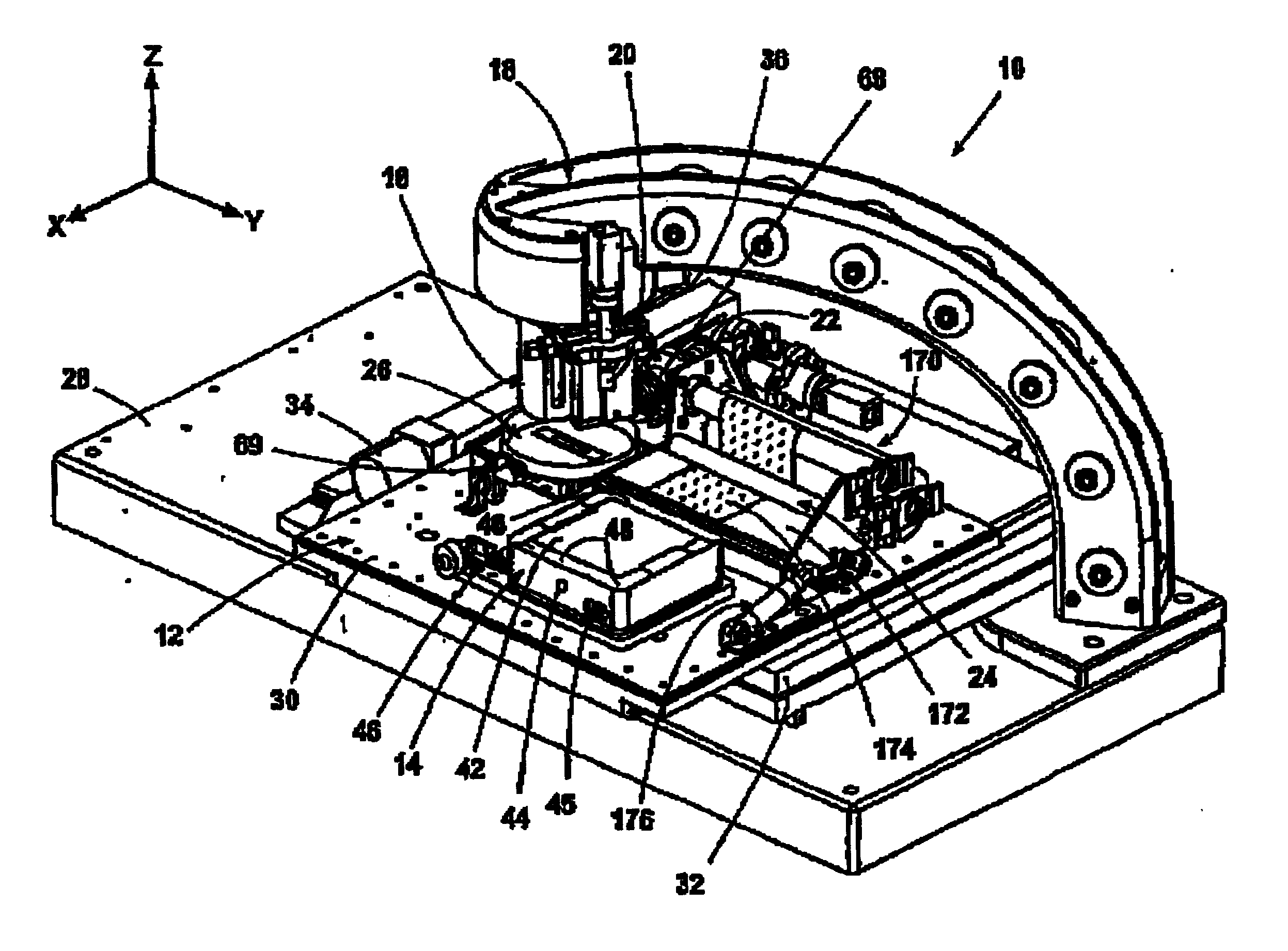
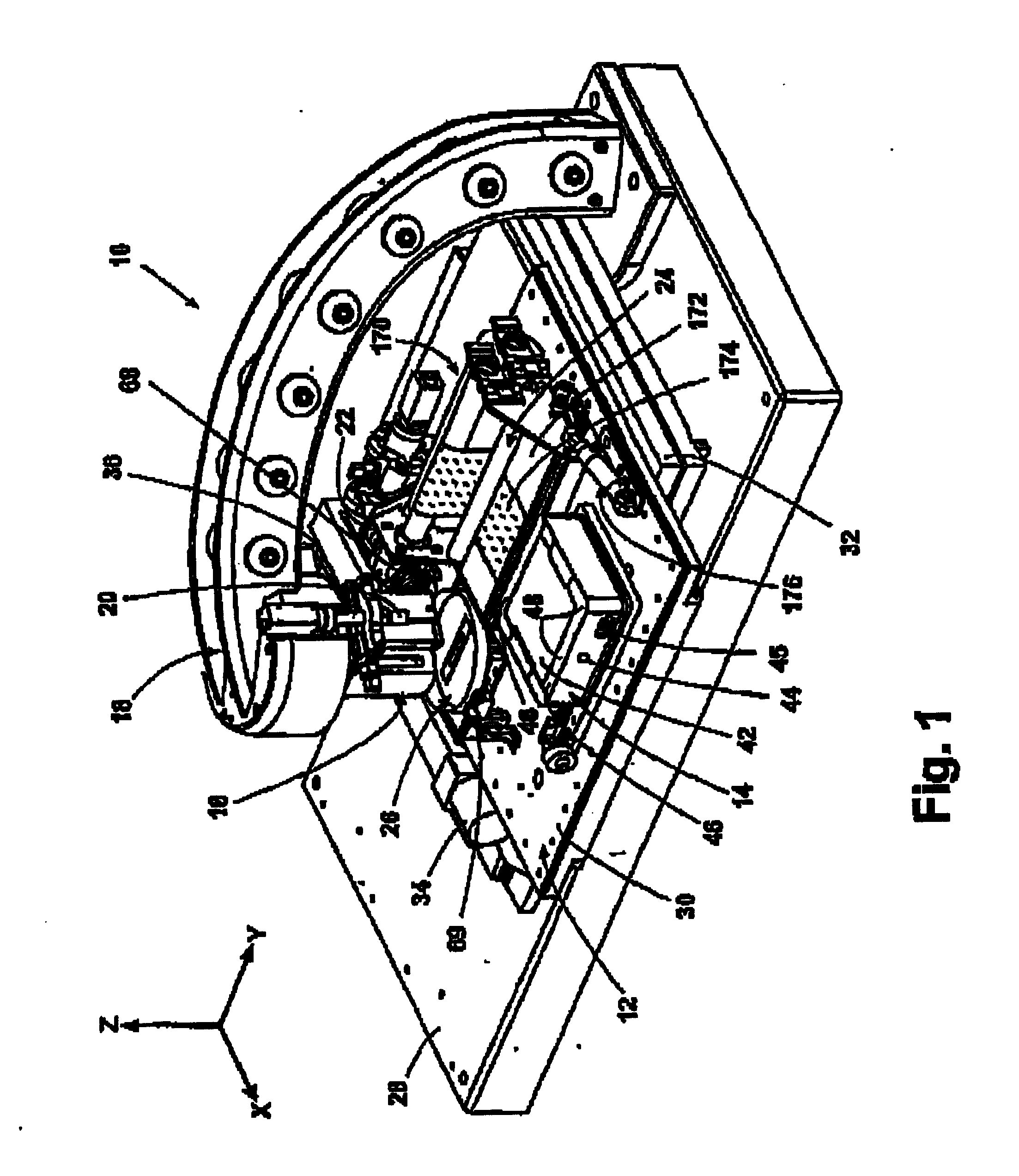
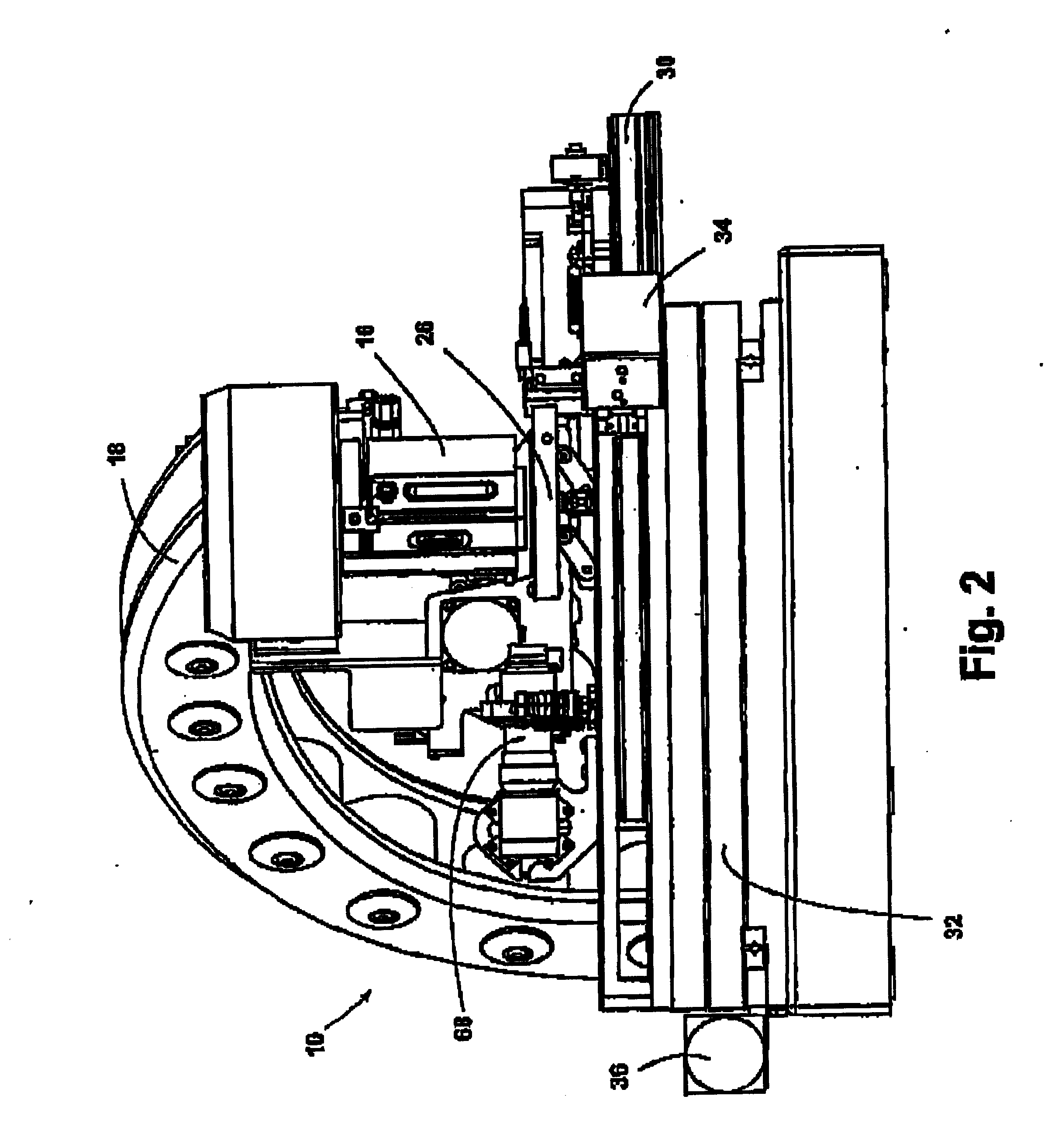
[0030] The present invention is directed to Piezoelectric Micro Deposition (PMD) of fluid manufacturing materials on substrates in controlled quantities and placements to manufacture or create microstructures.

[0031] The terms “fluid manufacturing material” and “fluid material” as defined herein, are broadly construed to include any material that can assume a low viscosity form and which is suitable for being deposited from a PMD head onto a substrate for forming a microstructure. Fluid manufacturing materials may include, but are not limited to, light-emitting polymers (LEPs), which can be used to form polymer light-emitting diode display devices (PLEDs, and PolyLEDs). Fluid manufacturing materials may also include plastics, metals, waxes, solders, solder pastes, biomedical products, acids, photoresists, solvents, adhesives and epoxies. The term “fluid manufacturing material” is interchangeably referred to herein as “fluid material.”

[0032] The term “deposition” as defined herein, g...


PUM

PropertyMeasurementUnit
diameteraaaaaaaaaa
volumeaaaaaaaaaa
velocityaaaaaaaaaa

Abstract

A microdeposition apparatus and method according to the invention includes an interchangeable microdeposition head for depositing fluid manufacturing material on a substrate to form microstructures. The apparatus includes at least one of a plurality of microdeposition heads mounted on a head support and held above a substrate, which is mounted on a stage in controlled alignment with the microdeposition head. The control system coordinates the relative movement of the stage and microdeposition head while the fluid manufacturing material is discharged from the microdeposition head. A mounting bracket and computer system enable various microdeposition heads to be interchangeably used with the microdeposition apparatus.

Description

CROSS-REFERENCE TO RELATED APPLICATIONS [0001] This application claims the benefit of U.S. Provisional Patent Application Ser. No. 60 / 295,118, entitled “Formation of Microstructures Using Piezo Deposition of Liquid Onto Substrate,” filed Jun. 1, 2001, and U.S. Provisional Application Ser. No. 60 / 295,100, entitled Formation Of Printed Circuit Board Structures Using Piezo Deposition Of Liquid Onto Substrate, filed Jun. 1, 2001, each of which is incorporated herein by reference.DISCUSSION OF THE INVENTION [0002] The present invention relates to methods and systems for forming microstructures on substrates and, more specifically, to methods and systems for performing piezoelectric microdeposition (PMD) of fluid manufacturing materials using interchangeable microdeposition tools. [0003] Manufacturers have developed various techniques for creating microstructures on substrates such as light-emitting diode (LED) display devices, liquid crystal display (LCD) devices, printed circuit boards ...

Claims


Application Information

Patent Timeline
Patent Type & Authority Applications(United States)
IPC IPC(8): B29C67/00B41J2/045B41J3/54H01L21/00H05K3/12
CPCB29C67/0059B41J2/04505B41J2/0451B41J2/04558B41J2/0456H05K3/125B41J2/04575B41J2/04581B41J2/04591B41J3/543H01L21/6715B41J2/04573B29C64/112
Inventor EDWARDS, CHARLES O.ALBERTALLI, DAVIDMIDDLETON, JAMESSLADE, BOYD
Owner LITREX CORP
Why Eureka
Try Eureka