High-speed, precision, laser-based method and system for processing material of one or more targets within a field

a laser-based, high-speed technology, applied in the direction of solid-state device testing/measurement, discharge tube/lamp details, solid-state device testing/measurement, etc., can solve the problems of limiting process quality, increasing the potential for substrate damage, and limited system throughpu

Inactive Publication Date: 2005-01-27
ELECTRO SCI IND INC
View PDF30 Cites 73 Cited by
  • Summary
  • Abstract
  • Description
  • Claims
  • Application Information

AI Technical Summary

Problems solved by technology

In many laser-processing applications, system throughput is limited by the average power, the substrates' fluence damage threshold, and, in pulsed systems, the laser q-rate and the laser pulse characteristics.
While smaller spots allow finer pitched fuses to be processed, the potential for substrate damage can increase with the higher fluence of a decreasing spot size as shown in FIG. 19b.
Laser trimming applications requiring a wide kerf width may require multiple passes with a small spot when the peak fluence of a larger spot is inadequate.
Out-of-round spots are often considered as system defects that limit process quality.

Method used


Image

  • High-speed, precision, laser-based method and system for processing material of one or more targets within a field
  • High-speed, precision, laser-based method and system for processing material of one or more targets within a field
  • High-speed, precision, laser-based method and system for processing material of one or more targets within a field

Examples


Embodiment Construction

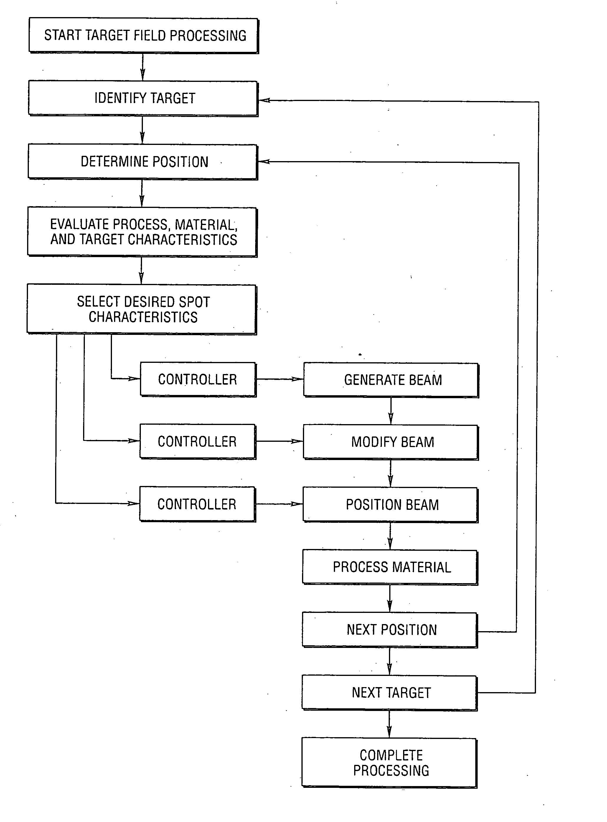
[0098] An aspect of the present invention involves laser processing of targets with a modified beam where spatial characteristics including aspect ratio of a spot are adjusted so that laser-material processing is performed in a desirable manner. Exemplary applications include, but are not limited to semiconductor link blowing, resistor trimming, laser drilling and various spot transformations.

[0099] For instance, the laser beam orientation and irradiance distribution may be substantially matched to the target geometry (e.g., FIGS. 19a-19d, a metal link 100 having a rectangular cross-section on a memory device) so as to efficiently couple the laser energy to the target (i.e., FIG. 19c) while reducing the background irradiance (e.g., Silicon substrate) and potential collateral damage. Such damage might occur through misalignment (FIG. 19d) or by overfilling with a round spot (FIG. 19a) where an adjacent link is irradiated. Though the situation in FIG. 19a appears extreme in the illus...


PUM

PropertyMeasurementUnit
aspect ratioaaaaaaaaaa
thicknessaaaaaaaaaa

Abstract

A precision, laser-based method and system for high-speed, sequential processing of material of targets within a field are disclosed that control the irradiation distribution pattern of imaged spots. For each spot, a laser beam is incident on a first anamorphic optical device and a second anamorphic optical device so that the beam is controllably modified into an elliptical irradiance pattern. The modified beam is propagated through a scanning optical system with an objective lens to image a controlled elliptical spot on the target. In one embodiment, the relative orientations of the devices along an optical axis are controlled to modify the beam irradiance pattern to obtain an elliptical shape while the absolute orientation of the devices controls the orientation of the elliptical spot.

Description

CROSS-REFERENCE TO RELATED APPLICATIONS AND PATENTS [0001] This application claims the benefit of U.S. provisional application Ser. No. 60 / 279,644, filed Mar. 29, 2001, entitled “Method and System for Severing Highly Conductive Micro-Structures.” This application is also related to U.S. patent application Serial No., filed on the same day as this application, and entitled “Method and System for Processing One or More Microstructures of a Multi-Material Device.” This application hereby incorporates the following U.S. patents by reference herein: U.S. Pat. Nos. 5,300,756; 6,144,118; 6,181,728; and 5,998,759.BACKGROUND OF THE INVENTION [0002] 1. Field of the Invention [0003] The present invention relates to the field of laser material processing methods and systems, and specifically, to scanned laser processing methods and systems for the processing of semiconductor wafers, electronic substrates, and workpieces to be laser micromachined. [0004] 2. Background Art [0005] Conventionally, ...

Claims


Application Information

Patent Timeline
Patent Type & Authority Applications(United States)
IPC IPC(8): B23K26/00B23K26/03B23K26/04B23K26/06B23K26/067B23K26/073B23K26/36B23K26/38B23K26/40B23K101/40G11C29/04H01L21/304H01L21/48H01L21/66H01L21/768H01L21/82H01L23/525H05K3/00
CPCB23K26/032B23K26/04H01L2924/0002B23K26/0613B23K26/063B23K26/0635B23K26/0639B23K26/0643B23K26/0648B23K26/0652B23K26/0665B23K26/067B23K26/0736B23K26/0807B23K26/10B23K26/16B23K26/365B23K26/386B23K26/4005B23K26/401B23K26/4015B23K26/402B23K26/4075B23K26/409B23K2201/38B23K2201/40B23K2203/08B23K2203/10B23K2203/12H01L21/485H01L21/76888H01L21/76894H01L22/12H01L23/5258H05K3/0026B23K26/043H01L2924/00B23K26/40B23K26/0622B23K26/0624B23K26/064B23K26/082B23K26/361B23K26/389B23K2101/38B23K2101/40B23K2103/10B23K2103/12B23K2103/172B23K2103/50H01L21/82
Inventor EHRMANN, JONATHAN S.CORDINGLEY, JAMES J.SMART, DONALD V.SVETKOFF, DONALD J.
Owner ELECTRO SCI IND INC
Why Eureka
Try Eureka