Measuring method and measuring apparatus of optical energy absorption ratio, and thermal processing apparatus

a technology of optical energy absorption and measuring apparatus, which is applied in the direction of instruments, semiconductor/solid-state device testing/measurement, furnaces, etc., can solve the problems of enormous optical energy irradiation to the wafer surface in an extremely short period of time, and the insufficient diffusion time of ions, so as to prevent damage to the substrate of processing objects during thermal processing

a technology of optical energy absorption and measuring apparatus, which is applied in the direction of instruments, semiconductor/solid-state device testing/measurement, furnaces, etc., can solve the problems of enormous optical energy irradiation to the wafer surface in an extremely short period of time, and the insufficient diffusion time of ions, so as to prevent damage to the substrate of processing objects during thermal processing

US20050018196A1Active Publication Date: 2005-01-27DAINIPPON SCREEN MTG CO LTD

Image

  • Measuring method and measuring apparatus of optical energy absorption ratio, and thermal processing apparatus
  • Measuring method and measuring apparatus of optical energy absorption ratio, and thermal processing apparatus
  • Measuring method and measuring apparatus of optical energy absorption ratio, and thermal processing apparatus

Examples


Embodiment Construction

Preferred embodiments of the present invention are now described in detail by referring to the accompanying drawings.

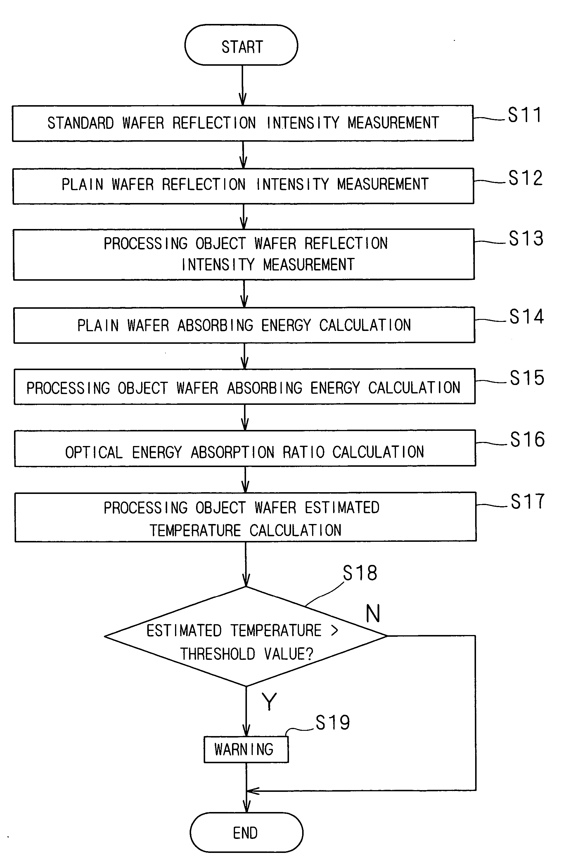
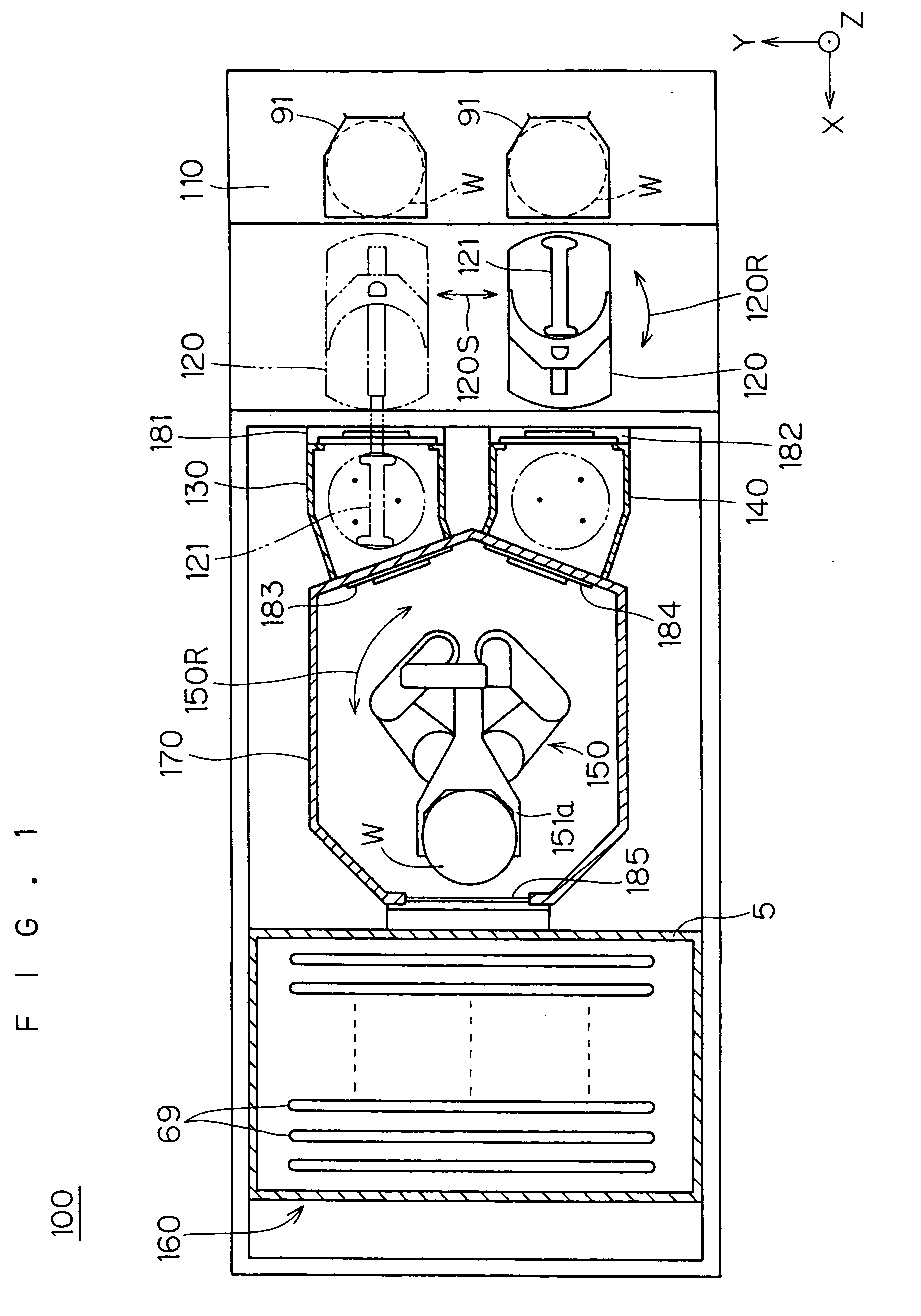
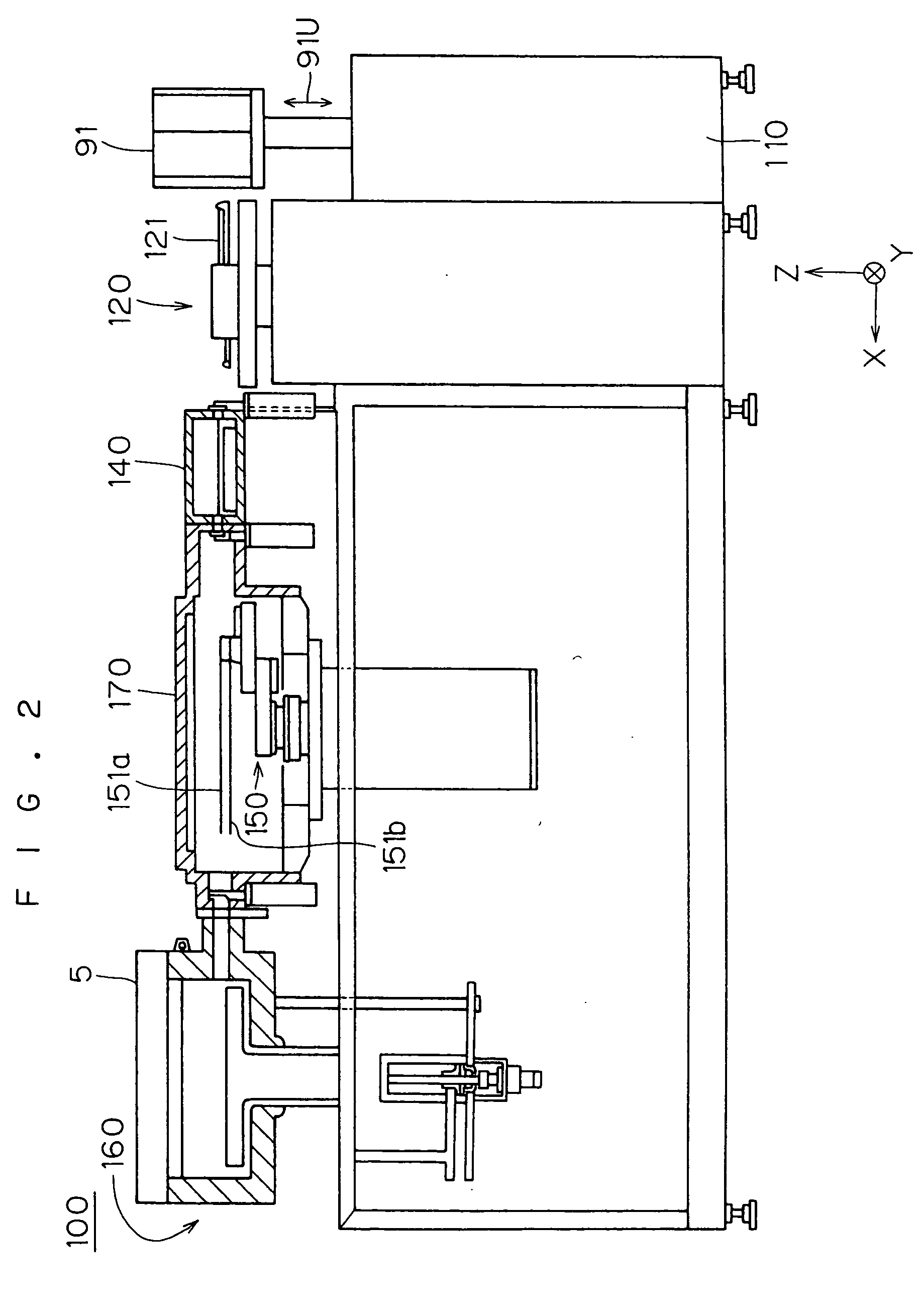
1. First Preferred Embodiment FIG. 1 and FIG. 2 are a plan view and a front view of a thermal processing apparatus 100 according to the present invention, respectively. For purposes of convenience, FIGS. 1 and 2 are partially sectioned, and the details are shown in simplified form. In order to clarify the directional relationship in FIGS. 1, 2, and the rest, where necessary, an XYZ rectangular coordinate system is appended, wherein the Z-axis direction is a vertical direction and an XY plane is a horizontal plane.

Referring to FIGS. 1 and 2, the thermal processing apparatus 100 has a substrate storing part (indexer) 110, on which two carriers 91 are mounted; a transfer robot 120 for loading and unloading a semiconductor wafer W with respect to the substrate storing part 110; an alignment part (aligner) 130 for aligning an untreated semiconductor wafer W; a cooling...


PUM


Abstract

Reflection intensities of a standard wafer with a known reflectance, a plain wafer on which no pattern is formed, and a semiconductor wafer to be processed practically are measured by using an optical measuring system. Their respective reflection intensities are subjected to spectral resolution processing. The optical energy value absorbed by the plain wafer is calculated from the reflection intensity of the standard wafer and the reflection intensity of the plain wafer. The optical energy value absorbed by the processing object wafer is calculated from the reflection intensity of the standard wafer and the reflection intensity of the processing object wafer. Based on these, the optical energy absorption ratio of the processing object wafer to the plain wafer is calculated. From this optical energy absorption ratio and the optimum energy value of light irradiated to the plain wafer, the optimum energy value to be irradiated to the processing object wafer is calculated.

Description

BACKGROUND OF THE INVENTION 1. Field of the Invention The present invention relates to a measuring method and a measuring apparatus for measuring optical energy absorption ratio of a processing object substrate to a plain substrate on which no pattern is formed, as well as a thermal processing apparatus employing such a measuring technique. 2. Description of the Background Art In an ion activation step of a semiconductor wafer after being subjected to ion implantation, there has heretofore been used a thermal processing apparatus such as a lamp annealing apparatus using halogen lamps. In such a thermal processing apparatus, the ion activation of a semiconductor wafer is carried out by heating (annealing) the semiconductor wafer to temperatures of, for example, approximately 1000° C. to 1100° C. This thermal processing apparatus is constructed so as to elevate the temperature of the substrate at a speed of about several hundreds of degrees per second, by utilizing the energy of l...

Claims


Application Information

Patent Timeline
27 Jan 2005
Publication
US20050018196A1
IPC
G01N21/27; G01N21/00; G01N21/31; H01L21/00; H01L21/26; H01L21/66
CPC
G01N21/31; H01L21/67248; H01L21/67115
Inventors
KUSUDA, TATSUFUMI