

Film thickness measuring method of member to be processed using emission spectroscopy and processing method of the member using the measuring method
- Summary
- Abstract
- Description
- Claims
- Application Information
AI Technical Summary
Benefits of technology
Problems solved by technology
Method used
Image

Examples
first embodiment
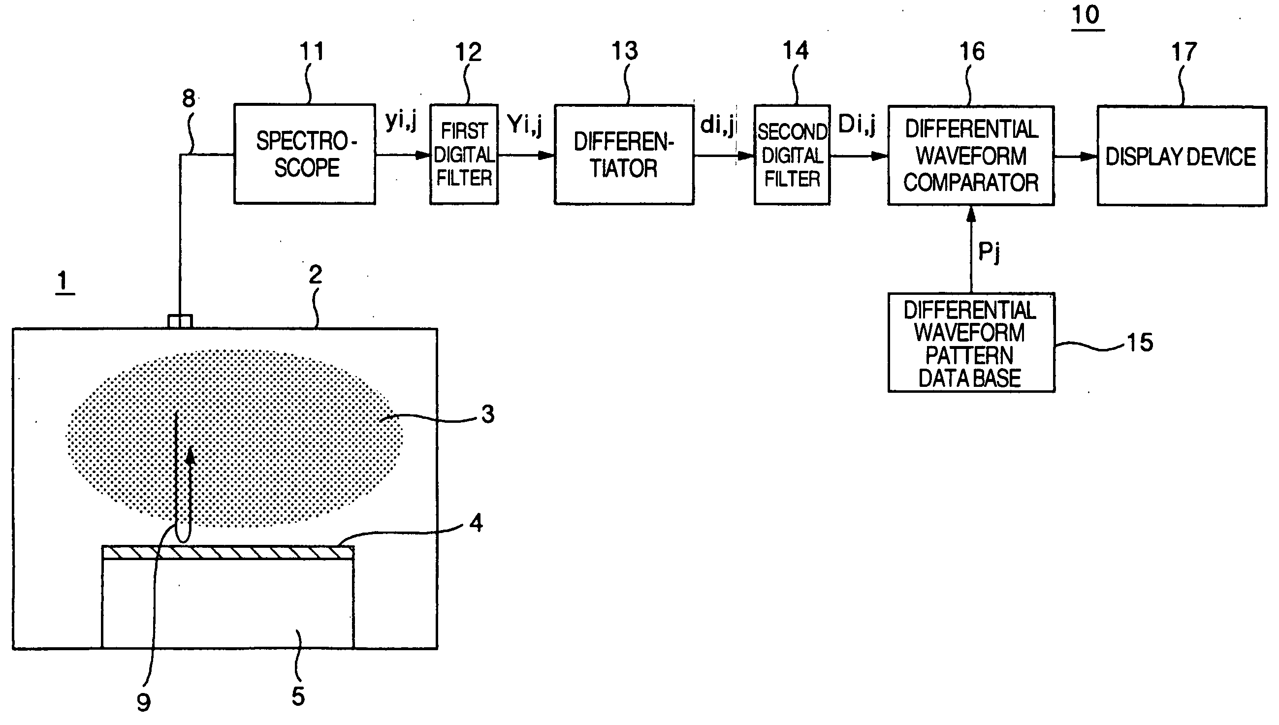
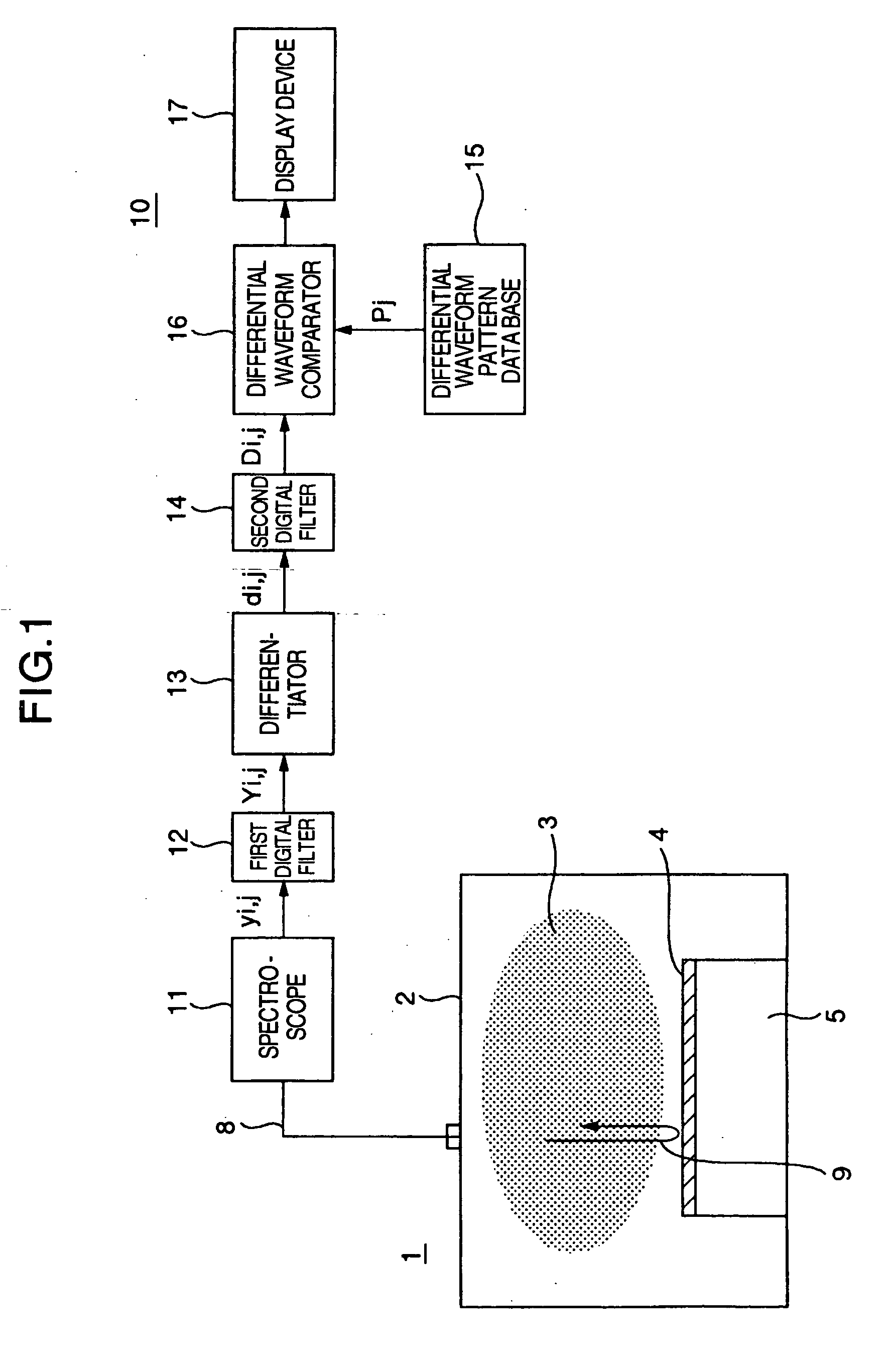
[0062] Hereunder, the preferred embodiments of the present invention will be described with reference to the accompanying drawings. In each of the embodiments, the same reference numbers will be given to the items having the same functions as those in the first embodiment, avoiding redundant description.
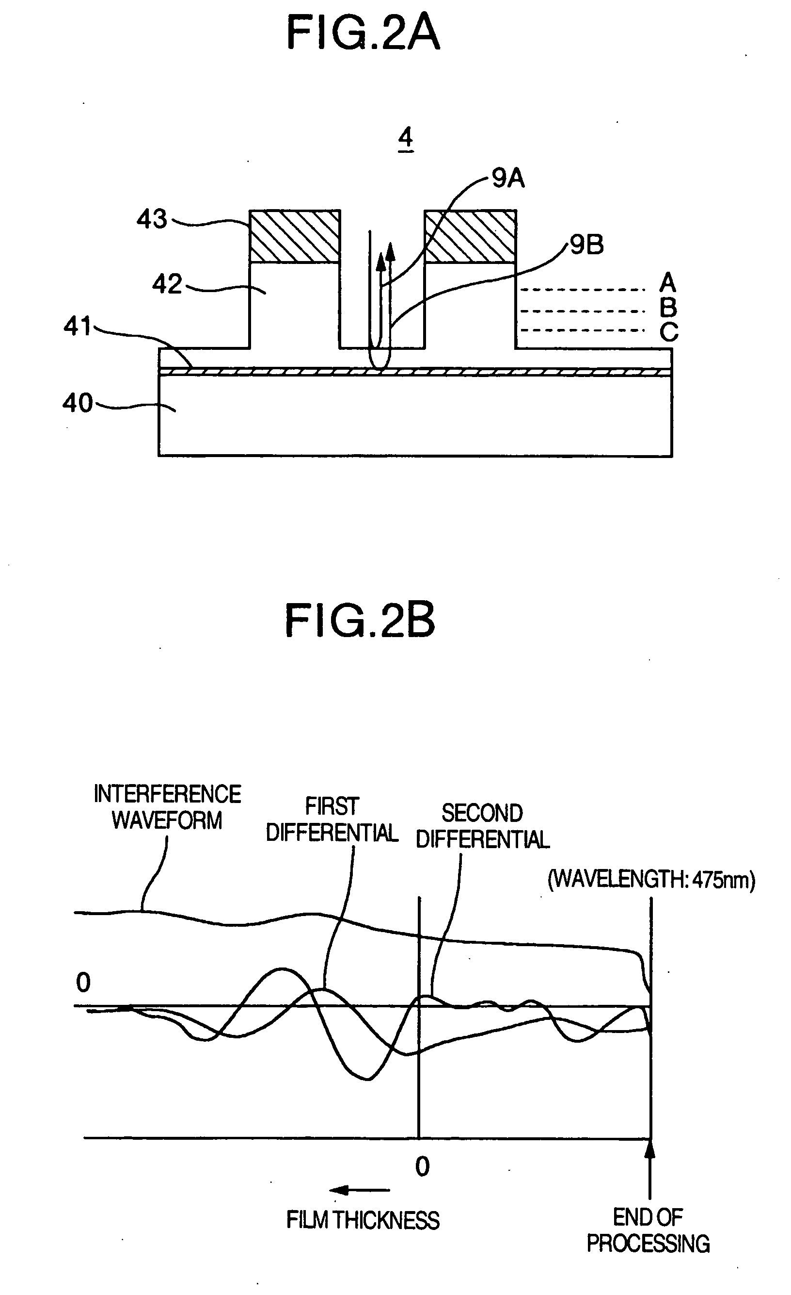
[0063] Hereinafter, the first embodiment of the present invention will be described with reference to FIGS. 1 through 4. In this first embodiment, a standard pattern denoting the wavelength dependence of a differential value of an interference light (a wavelength is used as a parameter) is set for plasma-etching of such members as wafers, etc. with respect to a predetermined film thickness of the sample member to be processed. Then, the intensity of an interference light is measured with respect to each of a plurality of its wavelengths in actual processing of a member composed just like the sample member. This is to find a real pattern denoting the wavelength dependence of a differe...
second embodiment
[0089] Next, the present invention will be described with reference to FIGS. 5 through 7. In this embodiment, it is possible to preset two conditions so as to detect that the film thickness of the subject member to be processed has reached to a predetermined value according to a standard pattern of a differential value corresponding to a predetermined film thickness. The two conditions are matching with a wavelength λ0 at one zero-cross point in this standard pattern and reaching of the matching rate between a differential value in another wavelength λp and the standard pattern of the actual value to the criterion σ0 or under.
[0090] In FIG. 5, a sampling signal having two specific wavelengths, output from the spectroscope 11, is stored in such a not-shown storage as a RAM as time series data yi, λo and yi, λp. Those time series data items are then smoothed by the first digital filter 12 and stored in a storage as smoothed time series data items Yi, λo, Yi, and λp. And, according to ...
third embodiment
[0100] Hereunder, the present invention will be described with reference to FIGS. 8 through 10. In this embodiment, a film thickness of a member to be processed is found from the number of zero-cross points n after a zero-cross pattern Pj of a differential value of a target wavelength λT is set and a zero-cross pattern of a differential value of an actual interference light intensity of the member is found in an interference light with respect to a predetermined film thickness of the member.
[0101] In FIG. 8, the sampling signal having a target wavelength of λT, output from the spectroscope 11, is stored as time series data yi,λT in such a storage (not illustrated) as a RAM. This time series data is then smoothed by the first digital filter 12 to smoothed time series data Yi,λT, which is stored in a storage. According to this smoothed time series data, the differentiator 13 calculates time series data di,λT of a differential value (first or second differential value), then stores the...
PUM
 Abstract
Description
Claims
Application Information