Current driver and display device

a current driver and display device technology, applied in the field of current drivers, can solve the problems of affecting the display quality, and deteriorating image quality, and achieve the effect of suppressing the variation of output current and suppressing uneven display

Active Publication Date: 2005-02-03
BISHOP DISPLAY TECH LLC
View PDF15 Cites 16 Cited by
  • Summary
  • Abstract
  • Description
  • Claims
  • Application Information

AI Technical Summary

Benefits of technology

[0016] Furthermore, a variation occurs in the current value among electric currents output from current drivers on different semiconductor chips. In many display devices, the production conditions, such as the dispersion condition, and the like, are different among a plurality of semiconductor chips arranged side by side. Therefore, a variation in the characteristics among the MISFETs which constitute the current sources of the current supply section 1001a1 is greater than that caused in the same chip, and accordingly, uneven display corresponding to respective semiconductor chips 1105 is likely to be seen. We thus concluded that suppressing a variation in output currents from an output terminal among the semiconductor chips 1105 is the most effective solution to suppress uneven display over a display panel.
[0017] An objective of the present invention is to provide a current driver capable of suppressing a variation in the output currents among a plurality of driver LSI chips that drive a display device, and a display device including such a current driver.

Problems solved by technology

However, in the display device having the above-described structure, a defect of image display, such as display unevenness, or the like, is sometimes seen during the display of images.
In such a case, in a semiconductor chip including a conventional current driver, there is a possibility that a variation occurs among the output currents from output terminals which are distant from each other, and as a result, deterioration in the image quality, such as uneven brightness in a displayed image, or the like, is caused.
However, in the case where the length of the driver LSI chips for a display device is as long as 10 mm to 20 mm, it is considered to be difficult to uniformly disperse impurities in the transistors.
In the case where a variation occurs among the threshold values of the transistors, an error occurs in the output current when the same gate voltage is applied to the transistors.

Method used


Image

  • Current driver and display device
  • Current driver and display device
  • Current driver and display device

Examples


embodiment 1

[0048] (Embodiment 1)

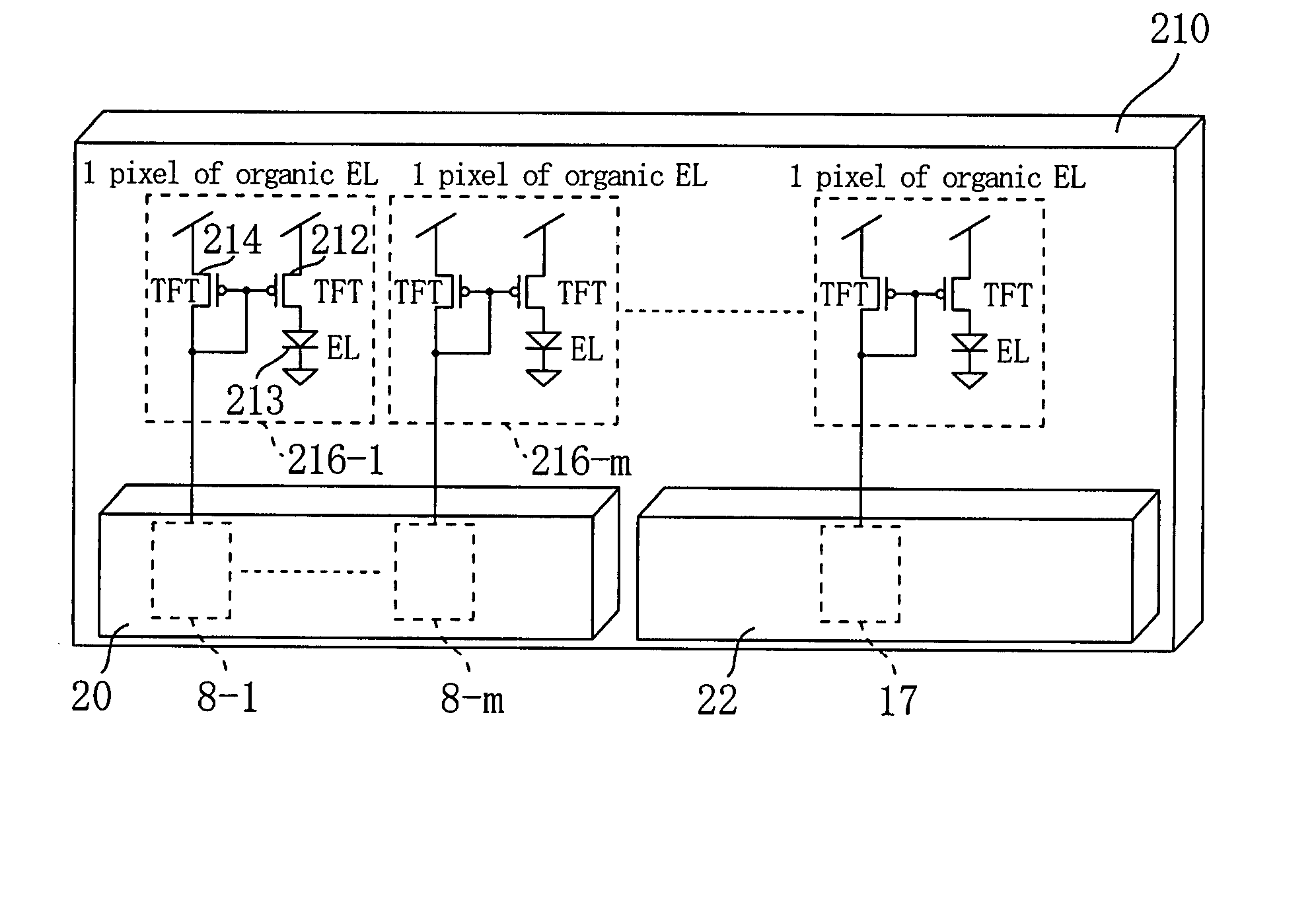
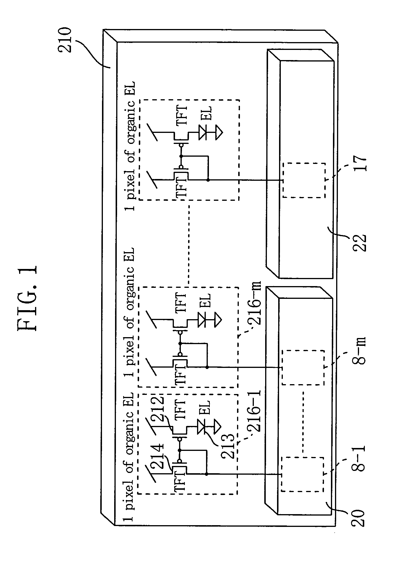
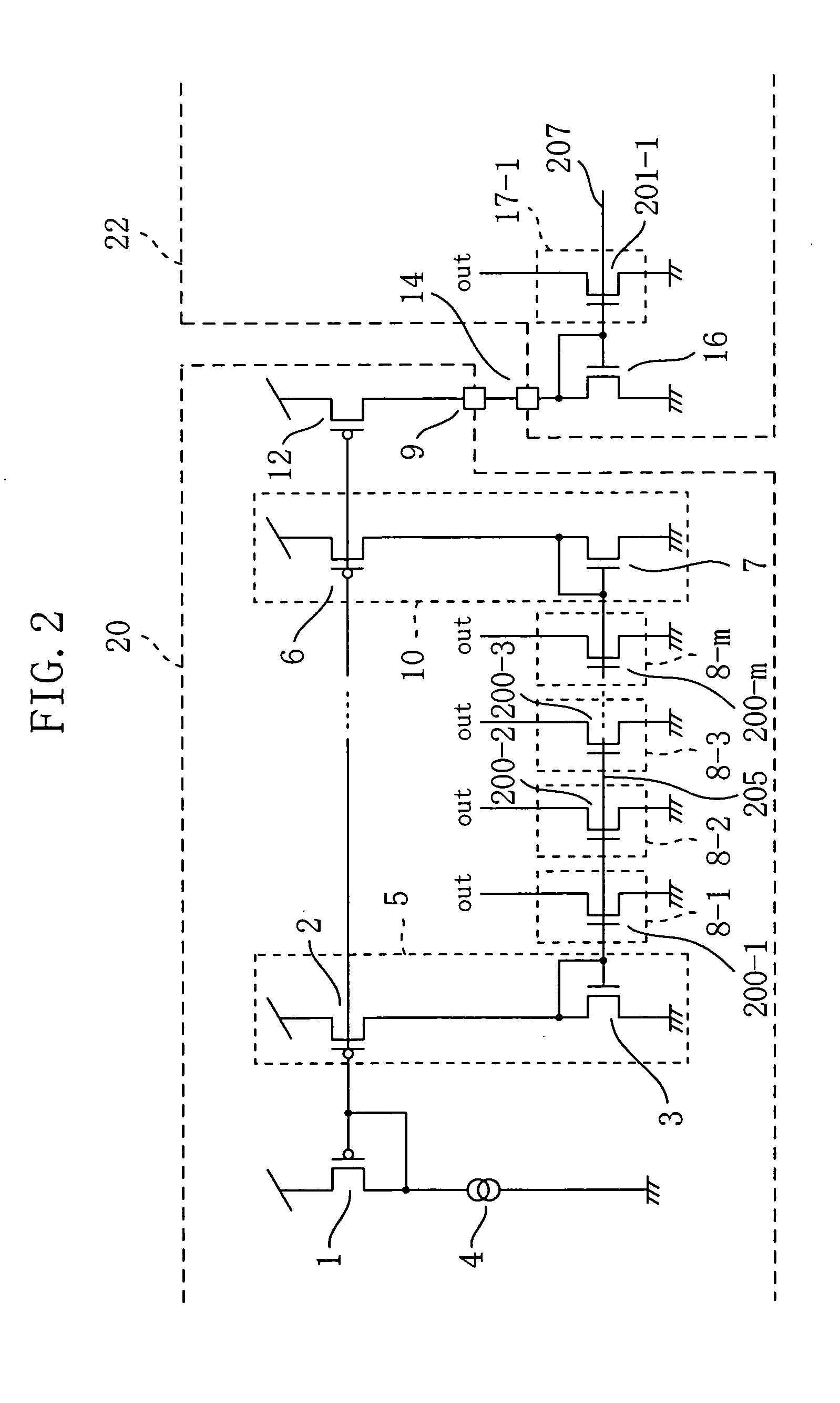
[0049]FIG. 2 is a circuit diagram showing semiconductor chips which include current drivers according to embodiment 1 of the present invention. The current drivers shown in FIG. 2 are used as source drivers of a current-driven display device, such as an organic EL display device, an LED display device, or the like, as are the current drivers of FIG. 14. In the example of FIG. 2, the first semiconductor chip 20 is a master chip, and the second semiconductor chip 22 provided adjacent to the first semiconductor chip 20 is a slave chip. These two chips are provided in the display device.

[0050] A first current driver is provided on the first semiconductor chip 20 of embodiment 1. The first current driver includes a plurality of first current supply sections 8, a reference current supply section for supplying the drive current (reference current) to the first current supply sections 8, a first bias circuit 5, a second bias circuit 10, a first current distribution MIS...

embodiment 2

[0065] (Embodiment 2)

[0066]FIG. 3 is a circuit diagram showing semiconductor chips which include current drivers according to embodiment 2 of the present invention. In FIG. 3, a first semiconductor chip 20, a second semiconductor chip 22 and a third semiconductor chip 24 are a master chip, a first slave chip, and a second slave chip, respectively, which are arranged in a line.

[0067] In embodiment 2, a current driver structure for performing current transmission equivalent to that described in embodiment 1 among three or more semiconductor chips is described. In FIG. 3, like elements are denoted by like reference numerals used in FIGS. 1 and 2 of embodiment 1, and descriptions thereof are herein omitted.

[0068] The first current driver is provided on the first semiconductor chip 20. The second current driver is provided on the second semiconductor chip 22. The third current driver is provided on the third semiconductor chip 24. The second semiconductor chip 22 and the third semicond...

embodiment 3

[0077] (Embodiment 3)

[0078]FIG. 4 is a circuit diagram showing semiconductor chips which include current drivers according to embodiment 3 of the present invention. In FIG. 4, a first current driver is provided on a first semiconductor chip 20, and a second current driver is provided on a second semiconductor chip 22.

[0079] The first and second current drivers of embodiment 3 are variations of the current drivers of embodiment 1. Hereinafter, differences in the first and second current drivers between embodiment 3 and embodiment 1 are described.

[0080] The first current driver of embodiment 3 includes, in addition to the components of the first current driver of embodiment 1, a sixth current distribution MISFET (additional current distribution MISFET) 36 of p-channel type and a third current output terminal 37 which is connected to the drain of the sixth current distribution MISFET 36. The gate electrode of the sixth current distribution MISFET 36 is connected to the first current ...


PUM


Abstract

The first and second chips are provided side by side. The first chip includes: a current supply section for outputting a drive current, the current supply section including a current mirror; a current distribution MISFET; a current input MISFET for transmitting an electric current to the current supply section, the current input MISFET being connected to the current distribution MISFET; and a second current distribution MISFET. The current distribution MISFET and the second current distribution MISFET constitute a current mirror. The second chip includes a second current input MISFET which is connected to the second current distribution MISFET. The ratio between the W/L ratio of the current distribution MISFET and the W/L ratio of the current input MISFET connected thereto is the same in the first and second chips.

Description

CROSS-REFERENCE TO RELATED APPLICATION [0001] This nonprovisional application claims priority under 35 U.S.C. § 119(a) on Japanese Patent Application No. 2003-281848, the entire contents of which are hereby incorporated by reference. BACKGROUND OF THE INVENTION [0002] 1. Field of the Invention [0003] The present invention relates to a current driver and particularly to a technology of current drivers suitable as a display driver for a display device, such as an organic EL (electroluminescent) panel, and the like. [0004] 2. Description of the Prior Art [0005] In recent years, in the fields of flat panel displays, such as organic EL panels, and the like, the screen size and definition have been increasing while the thickness, weight and production cost have been decreasing. In general, the active matrix method has been favorably employed as a method for driving a large, high-definition display panel. Hereinafter, a display driver for a conventional active matrix display panel is descr...

Claims


Application Information

Patent Timeline
Patent Type & Authority Applications(United States)
IPC IPC(8): H01L51/50G09G3/20G09G3/30G09G3/32H03B21/00H05B33/14
CPCG09G3/3241G09G3/3283G09G2330/028G09G2320/0233G09G2310/027G09G3/30
Inventor DATE, YOSHITOOMORI, TETSURODOSHO, SHIROMIZUKI, MAKOTO
Owner BISHOP DISPLAY TECH LLC
Why Eureka
Try Eureka