Method of forming multilayer interconnection structure, and manufacturing method for multilayer wiring boards

a manufacturing method and interconnection technology, applied in the direction of resist details, semiconductor/solid-state device details, printed circuit manufacturing, etc., can solve the problems of increasing contact resistance or non, increasing the degree of thinning of the film, and obtaining devices that may have a difference in electric characteristics, etc., to achieve high-reliability multi-layer wiring boards

Inactive Publication Date: 2005-02-03
SEIKO EPSON CORP
View PDF2 Cites 6 Cited by
  • Summary
  • Abstract
  • Description
  • Claims
  • Application Information

AI Technical Summary

Benefits of technology

[0024] A manufacturing method for multilayer wiring boards of the present invention is characterized in that the multilayer wiring i

Problems solved by technology

However, when the contact hole is formed by etching, the obtained devices may have a difference in electric characteristics according to ununiformity in film thickness of the interlayer insulating film in which the contact hole is formed.
Particularly in the case of dry etching, since the etching selection ratio between the insulating material and the conductive material cannot be sufficiently ensured, the degree of thinning of the film increases.
Such thinning of the wiring layer on the lower layer side causes an increase in contact resistance or non-ohmic conduction characteristics, and sometimes causes insufficient conduction.
The enlarged shape of the contact hole due to over etching causes an increase in leak current between adjacent conductive layers or a short circuit failure.
The problem of leak current or short circuit becomes serious as the density of the wiring layer increases and the gaps between the adjacent wiring layers becomes narrower.
Moreover, in a portion where the film thickness is thick, the interlayer insulating film remai

Method used


Image

  • Method of forming multilayer interconnection structure, and manufacturing method for multilayer wiring boards
  • Method of forming multilayer interconnection structure, and manufacturing method for multilayer wiring boards
  • Method of forming multilayer interconnection structure, and manufacturing method for multilayer wiring boards

Examples


first embodiment

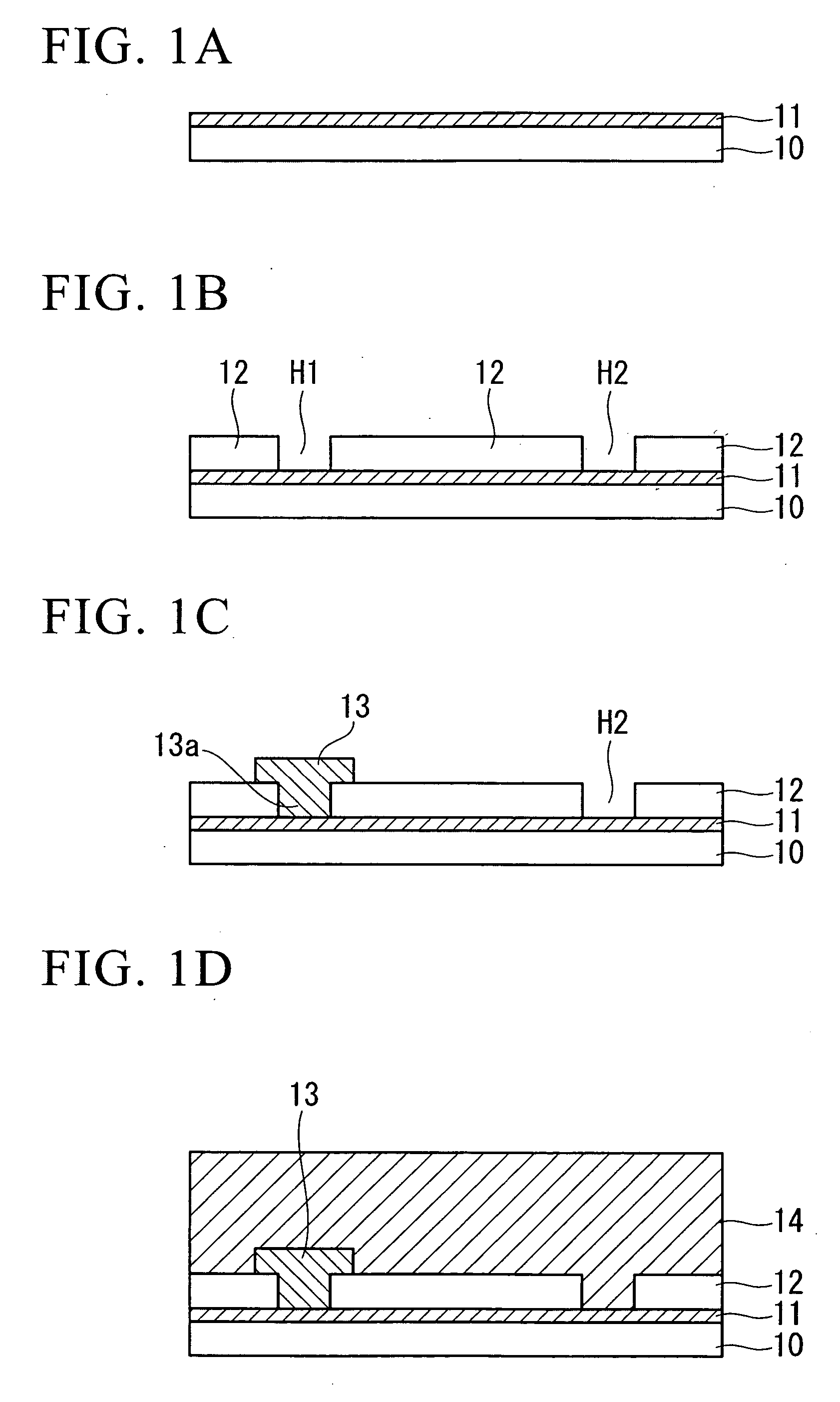
[0033] (First Embodiment)

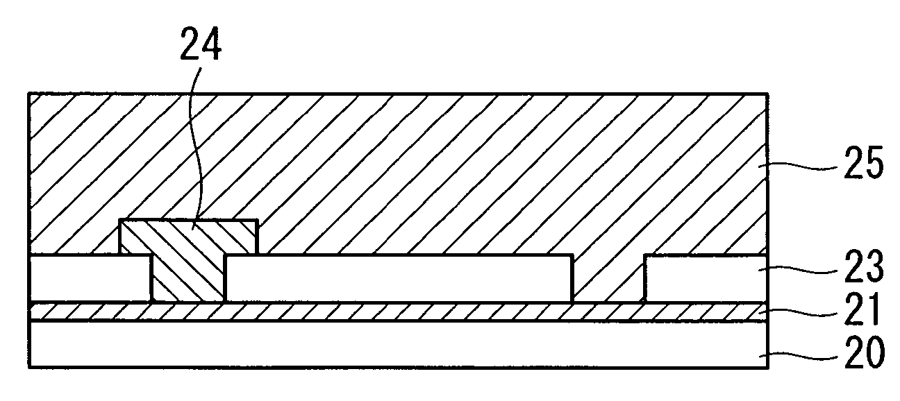
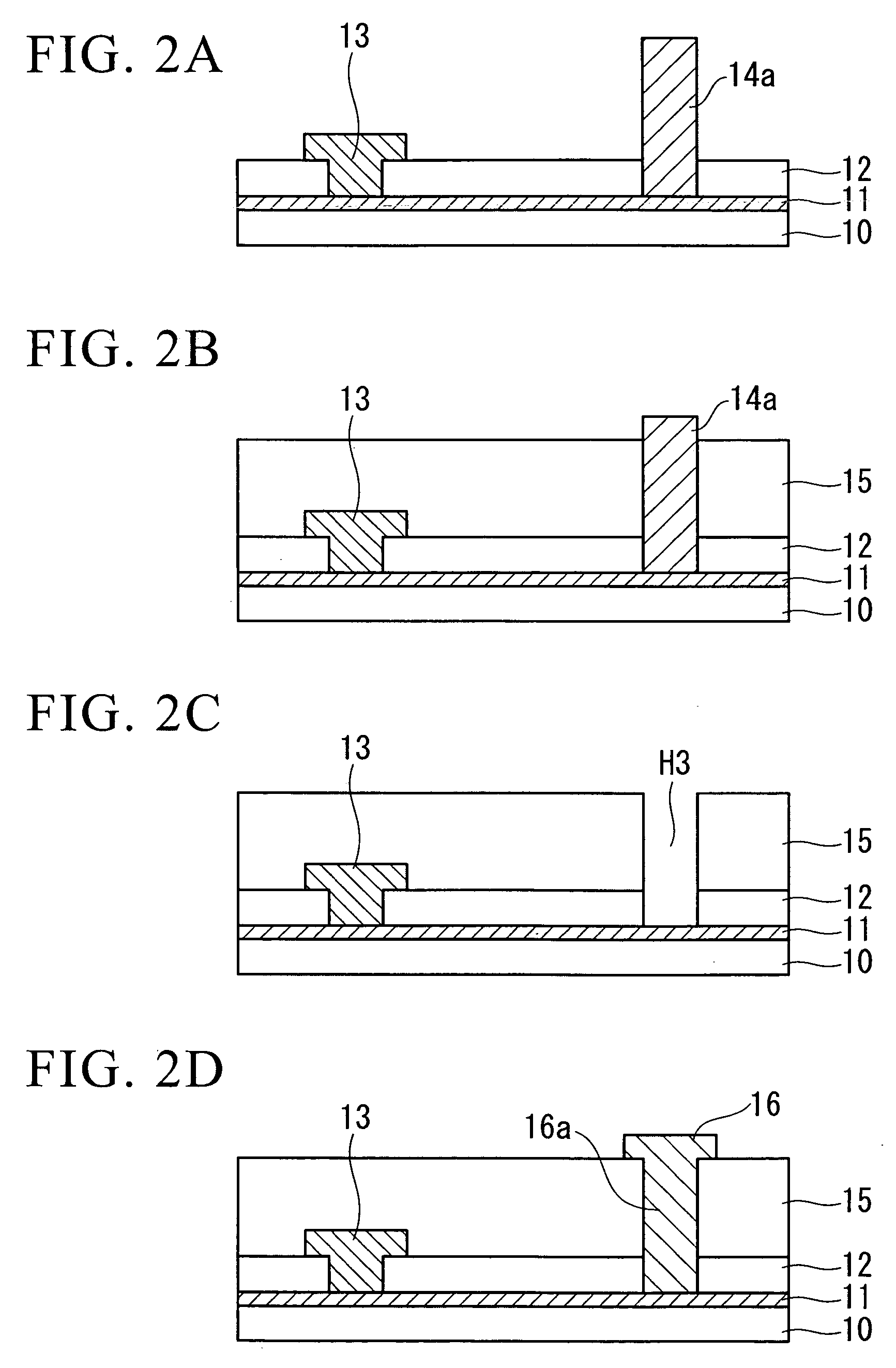
[0034] First is a description of a manufacturing method for multilayer wiring boards according to a first embodiment of the present invention, with reference to FIG. 1A to FIG. 2D. FIG. 1A to FIG. 2D show examples where the present invention is applied to a step of laminating three wiring layers on a substrate. In all drawings hereunder, the film thicknesses and dimensional proportions of the respective components are appropriately changed for clarity.

[0035] In the present embodiment, firstly as shown in FIG. 1A, a wiring layer 11 is formed on the surface of a substrate 10 such as a semiconductor substrate on which an insulating film is formed, or an insulating substrate made of glass or plastic, using a well-known method.

[0036] Next, as shown in FIG 1B, an interlayer insulating film 12 having openings H1 and H2 is formed in a predetermined position on the wiring layer 11. The interlayer insulating film 12 can be formed by a plasma CVD method using TEOS (t...

second embodiment

[0049] (Second Embodiment)

[0050] Next is a description of a method of forming a multilayer interconnection structure according to a second embodiment of the present invention, with reference to FIG. 3A to FIG. 5B. FIG. 3A to FIG. 5B show examples where the present invention is applied to a step of laminating three wiring layers on a substrate. In the present embodiment, the description is related to a method of forming a multilayer interconnection structure where a first layer and a third layer become conductive, the first layer and a second layer become conductive, and the second layer and the third layer become conductive.

[0051] In the present embodiment, firstly as shown in FIG. 3A, a wiring layer 21 is formed on the surface of a substrate 10 made of glass or plastic, using a well-known method. On the wiring layer 21, mask pillars (mask material) 22 are formed in positions for forming openings H4 and H5 described later. The mask pillars 22 are formed by selectively applying liqu...

third embodiment

[0063] (Third Embodiment)

[0064] Next is a description of a manufacturing method for multilayer wiring boards according to a third embodiment of the present invention, with reference to FIG. 6A to FIG. 8B. FIG. 6A to FIG. 7C show examples where the present invention is applied to a step of laminating three wiring layers on a substrate. In the present embodiment, the description is related to a method of forming a multilayer interconnection structure where a first layer and a third layer become conductive, and the first layer and a second layer become conductive.

[0065] In the present embodiment, firstly as shown in FIG. 6A, a wiring layer 31 is formed on the surface of a substrate 30 made of glass or plastic, using a well-known method. On the wiring layer 31, a mask pillar (mask material) 32 is formed in the position for forming an opening H8 described later. The mask pillar 32 is formed by selectively applying liquid organic material such as a resist or the like and solidifying this...


PUM


Abstract

Method of forming a multilayer interconnection structure that includes a contact hole for reliably connecting between layers, without damaging a substrate. A column shaped mask material is formed in a position for forming a contact hole using a resist, and an interlayer insulating film is applied to the whole surface of the substrate excluding the mask material. Then, the mask material is removed by a method such as peeling. As a result, a hole generated thereby is used as a contact hole.

Description

PRIORITY CLAIM [0001] Priority is claimed on Japanese Patent Application No. 2003-282579, filed Jul. 30, 2003, the content of which is incorporated herein by reference. BACKGROUND OF THE INVENTION [0002] 1. Field of the Invention [0003] The present invention relates to a method of forming a multilayer interconnection structure, and a manufacturing method for multilayer wiring boards, and more specifically, relates to a contact hole formation technique for connecting between wiring layers. [0004] 2. Description of the Related Art [0005] Recently, in electronic devices such as semiconductor devices and electro-optic devices, wiring is formed in multi layers in order to increase the degree of integration. In devices having such a multi-layer wiring structure, a contact hole (opening) is formed in an interlayer insulating film, in order to secure conduction between wiring layers laminated via the interlayer insulating film. [0006] For example, in a field of electro-optic devices, one in...

Claims


Application Information

Patent Timeline
IPC IPC(8): H01L21/00H01L21/02H01L21/288H01L21/28H01L21/3205H01L21/4763H01L21/768H01L29/786H05K3/00H05K3/46
CPCH01L21/76802H05K2203/0582H05K3/4644H05K3/0017
Inventor YUDASAKA, ICHIOSATO, MITSURU
Owner SEIKO EPSON CORP
Why Eureka
Try Eureka