

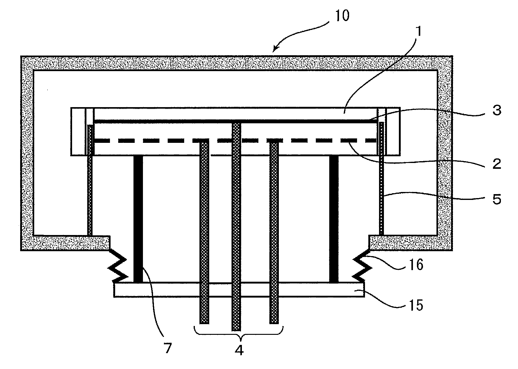
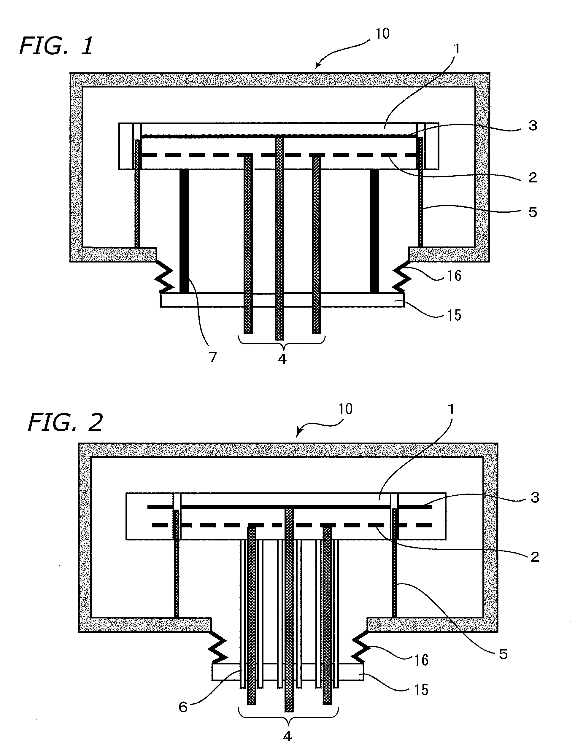
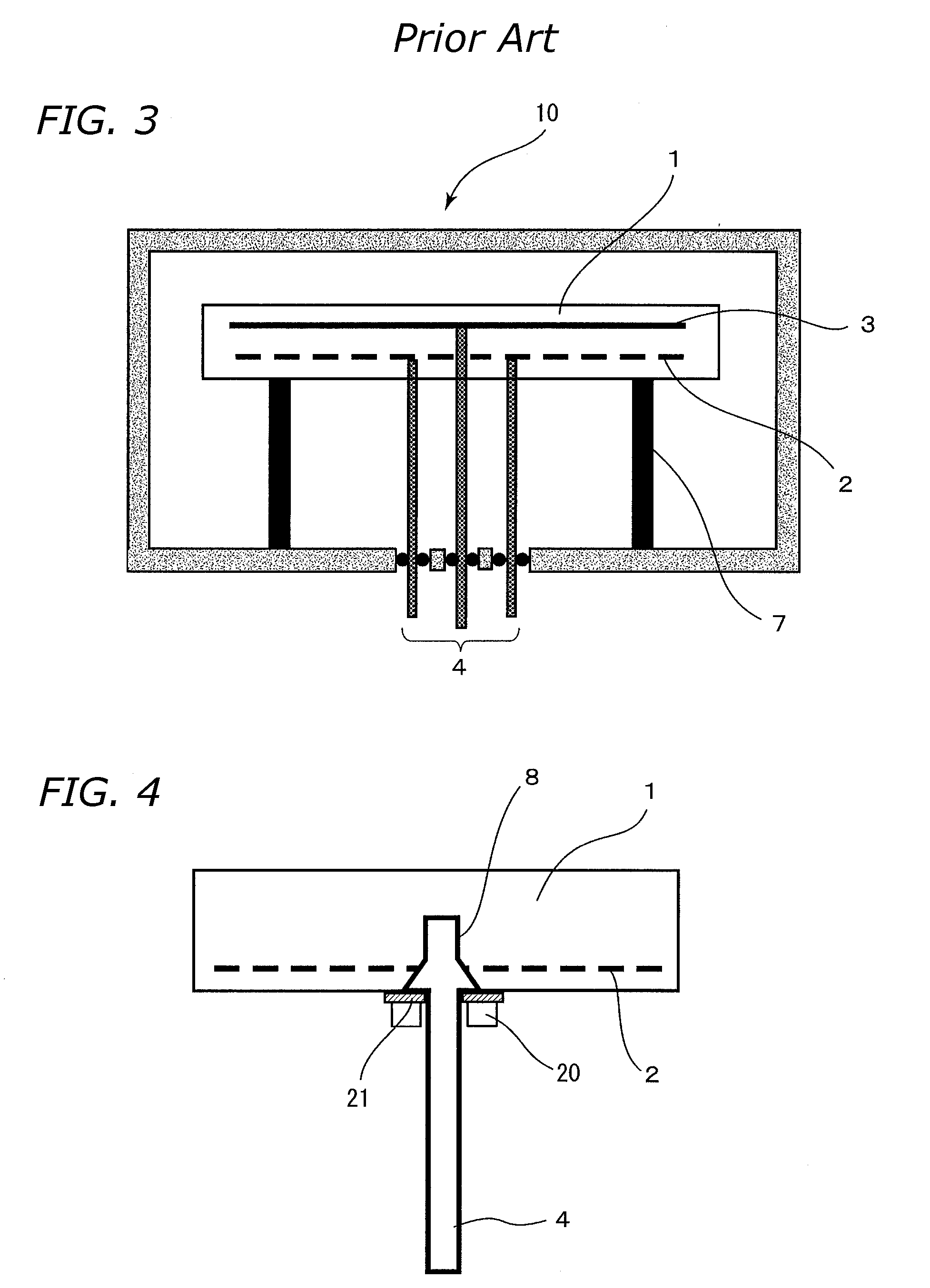
Semiconductor Manufacturing Apparatus
a manufacturing apparatus and semiconductor technology, applied in the direction of coatings, chemical vapor deposition coatings, metallic material coating processes, etc., can solve the problems of large volume of the chamber, plurality of lift pins, and large so as to achieve the effect of reducing the overall volume of the apparatus
- Summary
- Abstract
- Description
- Claims
- Application Information
AI Technical Summary
Benefits of technology
Problems solved by technology
Method used
Image

Examples
embodiment
[0081] Embodiment
[0082] 99.5 parts by weight aluminum nitride powder and 0.5 parts by weight Y2O3 powder were blended together; 10 parts by weight polyvinyl butyral as a binder and 5 parts by weight dibutyl phthalate as a solvent were added to the mixture, which was then mixed in a ball mill for 24 hours to prepare a slurry. Here, an aluminum nitride powder of 0.6 □m mean particle diameter and 3.4 m2 / g specific surface area was utilized. The slurry was granulated by spray-drying, and the granules were charged into a mold and molded to produce a molded part. After being degreased at 800° C., the molded part was sintered 6 hours at 1850° C. to yield a sintered AlN part. Here, the ambient during degreasing and sintering was made a nitrogen atmosphere.
[0083] Furthermore, a tungsten paste was prepared by adding, to 100 parts by weight tungsten powder of 2.0 □m mean particle diameter, Y2O3 powder at 1 part by weight, Al2O3 at 0.6 weight %, and ethyl cellulose—a binder—and butyl Carbitol™...
PUM
| Property | Measurement | Unit |
|---|---|---|
| Height | aaaaa | aaaaa |
Abstract
Description
Claims
Application Information