Semiconductor circuit and method of fabricating the same

a semiconductor and circuit technology, applied in the direction of semiconductor devices, electrical devices, transistors, etc., can solve the problems of reducing the production efficiency of semiconductor films, so as to reduce the variation between semiconductor circuits (analog circuits) and the plurality of semiconductor devices.

Inactive Publication Date: 2005-02-10
SEMICON ENERGY LAB CO LTD
View PDF66 Cites 32 Cited by
  • Summary
  • Abstract
  • Description
  • Claims
  • Application Information

AI Technical Summary

Benefits of technology

[0014] Another object of the present invention is to form a plurality of semiconductor devices which require high conformity from crystalline semiconductor films with uniform crystallinity, further to provide a semiconductor circuit in which variation between semiconductor devices is small and a semiconductor integrated circuit with high performance.
[0025] As the laser light or the strong light which is concentrated in a line shape and expanded in a long direction is irradiated to the semiconductor film, a position of laser light irradiation and a substrate on which the crystalline semiconductor films are formed move relatively, and the semiconductor films are melted by scanning a part or whole thereof by the laser light, and through that situation, crystallization or recrystallization is carried out. The scanning direction of the laser light is along a long direction of the depression formed in the insulating film and extending as a liner stripe pattern or a channel length direction of the transistor. By this, crystals are grown along the scanning direction of the laser light, and it is possible to prevent crystal grain boundaries from crossing the channel length direction.
[0028] By setting depth of the depression as the same level or more as thickness of the semiconductor film, the semiconductor film which is melted by irradiation of the laser light or the strong light is coagulated and solidified in the depression due to surface tension. As a result, the thickness of the semiconductor film located on the projection of the insulating film gets thinner so that it is possible to localize stress-strains on it. Also, a side surface of the depression has an effect for defining crystal orientation to some degree.
[0034] According to the invention, on the insulating surface, in particular, on the insulating surface in case that an inexpensive glass substrate is used as a support substrate, the channel forming regions are formed from the stripe-shaped crystalline semiconductor films on the same line so that variation between a plurality of semiconductor devices can be reduced, and further, variation between semiconductor circuits (analog circuits) can be reduced, and it is possible to provide a high-performance semiconductor integrated circuit. In addition, two or more semiconductor circuits gather to form the semiconductor integrated circuit, and the semiconductor circuit has semiconductor devices comprising thin film transistors in which at least conformity is required.

Problems solved by technology

However, when crystallization is made by irradiating the laser beams onto the amorphous semiconductor film, the crystal includes poly-crystals, producing defects such as a grain boundary which is formed at random.
Therefore, it becomes difficult to obtain uniform crystallinity and crystal orientations.
Crystal defects are involved in a grain boundary, resulting in a carrier trap.
Also, it is impossible to form a semiconductor film with neither distortion nor crystal defects due to a volume shrinkage of the semiconductor films, a thermal stress applied between the semiconductor film and a base film, or lattice mismatching, accompanied with crystallization.
Consequently, the distortion and crystal defects produce causative factors of not only variation of electrical characteristics of the semiconductor device, but also inferior electrical characteristics of the semiconductor device.
Especially when crystalline semiconductor films are formed by using laser beams on a non-alkali glass substrate used abundantly and industrially, the focuses of the laser beams varies in response to the influence of the surge of the non-alkali glass substrate itself, involving a problem of causing crystalline variation as a result.
The semiconductor integrated circuit and the like have semiconductor films formed on cheap glass substrates to constitute transistors, therefore, it is almost impossible to arrange transistors so as to aovid grain boundaries formed at random.
That is, the grain boundaris or crystal defects involved unexpectedly could not be eliminated by controlling strictly the crystallinity of the channel forming regions of transistors.
This produced a causative factor of variation of electrical characteristics of the semiconductor device, thus, it is difficult to form a circuit which requires high conformity (for example, a current mirror circuit).

Method used


Image

  • Semiconductor circuit and method of fabricating the same
  • Semiconductor circuit and method of fabricating the same
  • Semiconductor circuit and method of fabricating the same

Examples


example 1

[0174] This example describes a current mirror circuit and a differential amplifier circuit as an analog circuit which is formed by use of the invention.

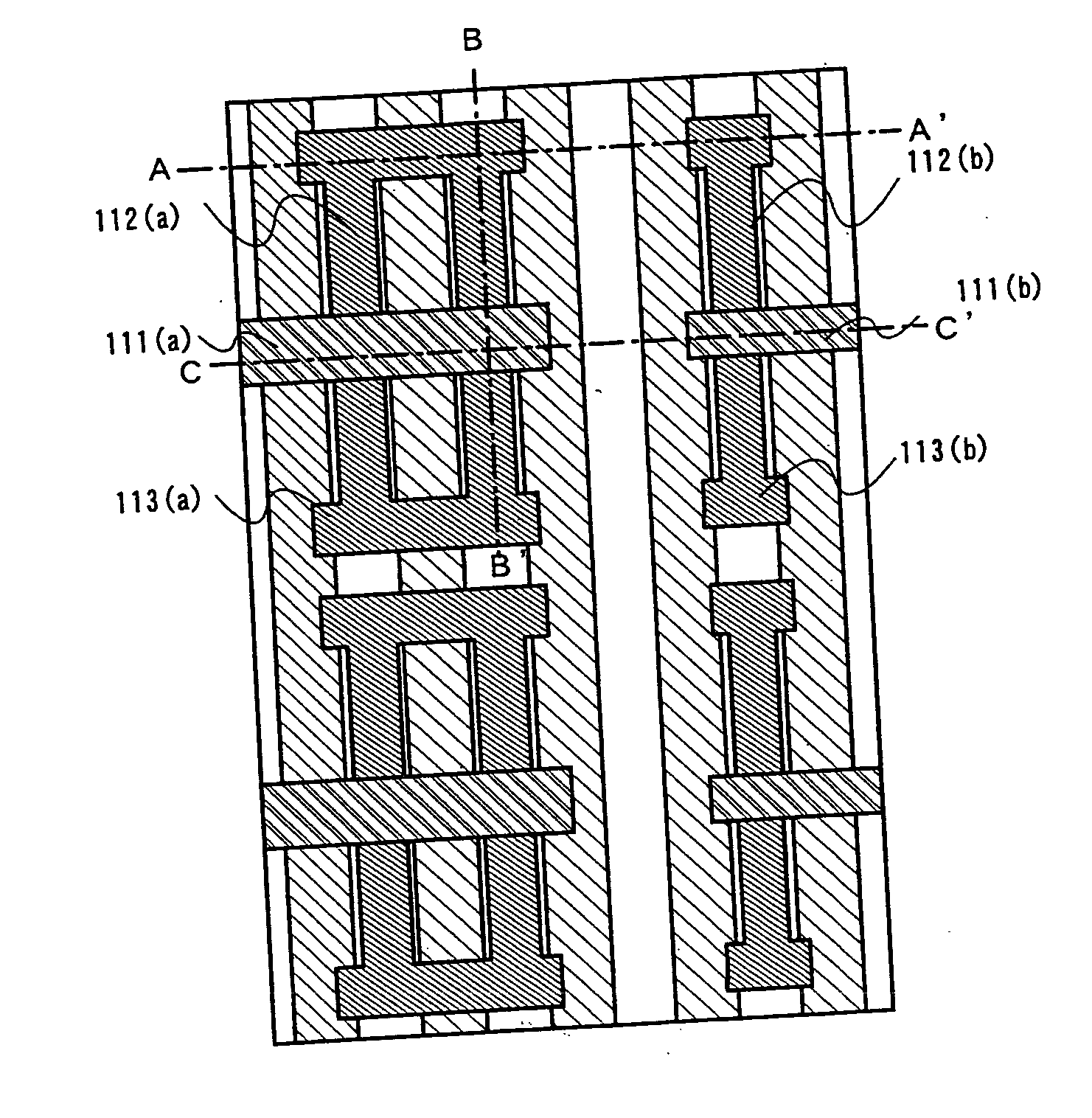
[0175]FIGS. 14A-1 and 14A-2 show an equivalent circuit diagram of the current mirror circuit and a top view of a layout example. In addition, polarities of thin film transistors 1510 and 1511 which the current mirror circuit has are of p-channel type by way of example.

[0176] Looking at FIG. 14A-1, a power line Vdd and drain electrodes of the thin film transistors 1510 and 1511 are connected, and the gate electrode of the thin film transistor 1510 and the gate electrode and the source electrode of the thin film transistor 1511 are connected, and the source electrode of the thin film transistor 1511 is connected to Vss through a current source. Thin film transistors which is required to have conformance are the thin film transistors 1510 and 1511 surrounded by the dotted line.

[0177] Also, looking at FIG. 14A-2, the gate electrode i...

example 2

[0188] This example will describe a circuit of an analog switch which is formed by the invention.

[0189]FIGS. 15A and 15B show equivalent circuit diagrams of neighboring two analog switches SW1 and SW2 (analog switches surrounded by a broken line) and a top view of a layout example. In addition, polarities of thin film transistors 1516 and 1518 which the two analog switches have are of p-channel type, and polarities of 1517 and 1519 are of n-channel type by way of example.

[0190] Thin firm transistors which are required to have conformance in the analog switch of this example are the thin film transistors 1516 and 1518, or the thin film transistors 1517 and 1519. Also, this example describes an example of the analog switch which is configured by two thin film transistors which are required to have conformance but, it goes without saying that the invention is not limited to one Which is configured by two thin film transistors.

[0191] Looking at FIG. 15A, a wiring to which an input si...

example 3

[0196] This invention can be applied to various semiconductor apparatuses, and the forms of a display panel produced based on the embodiments 1 to 5 and examples 1 to 2, will be explained. In addition, as an example of the display panel shown in this example, the display panel using a transistor as a semiconductor device, such as a liquid-crystal-display panel, an EL (Electro Luminescence) display panel, and a display panel for FED (Field Emission Display), are mentioned. Of course, these display panels include a module which is currently distributed in the market.

[0197] A substrate 900 of FIGS. 16A to 16C has a pixel part 902, gate signal side drive circuits 901a, 901b, a data signal side drive circuit 901c, an input-and-output terminal part, and a wiring, or a wiring group 917 formed thereon.

[0198] A seal pattern 940 is a pattern for making a sealed space between the opposite substrate 920 and the substrate 900, and in case of a liquid crystal display panel, liquid crystal is en...


PUM


Abstract

According to the invention, a plurality of semiconductor devices which are required to have conformance are formed from crystalline semiconductor films having uniform crystallinity on the same line, and a semiconductor circuit in which variation between semiconductor devices is small can be provided, and a semiconductor integrated circuit having high conformance can be provided. The invention is characterized in that, in a part or whole of thin film transistors which configure an analog circuit such as a current mirror circuit, a differential amplifier circuit, or an operational amplifier, in which high conformance is required for semiconductor devices included therein, channel forming regions have crystalline semiconductor films on the same line. High conformance can be expected for an analog circuit which has the crystalline semiconductor films on the same line formed using the invention as the channel forming regions of the thin film transistors. That is, the invention is characterized in that, among the thin film transistors which configures the analog circuit, the channel forming regions of the thin film transistors having at least the same polarity are formed on the same line.

Description

BACKGROUND OF THE INVENTION [0001] 1. Field of the Invention [0002] The present invention relates to a semiconductor device which is formed by using a semiconductor film having a crystal structure (also referred to as a crystalline semiconductor film) and a method for manufacturing the same, as well as a semiconductor integrated circuit equipped with a circuit integrating the semiconductor devices and a method for manufacturing the same. Further, the present invention relates to a semiconductor device having a plurality of the semiconductor integrated circuits. And, the present invention especially relates to a thin film transistor which forms a channel forming region by a crystalline semiconductor film formed on an insulating surface as a semiconductor device. [0003] 2. Description of the Related Art [0004] A technique for forming a semiconductor device such as a thin film transistor and the like using a crystalline semiconductor film formed on an insulation substrate such as glass...

Claims


Application Information

Patent Timeline
Patent Type & Authority Applications(United States)
IPC IPC(8): H01L21/336H01L21/77H01L21/84H01L27/12H01L29/786
CPCH01L21/2026H01L27/12H01L27/1281H01L29/78675H01L29/78696H01L29/66757H01L21/02686H01L21/0242H01L21/02683H01L21/02691H01L21/02425H01L21/02488H01L21/02422H01L21/02672H01L21/02532H01L21/02678H01L21/02502
Inventor KATO, KIYOSHIATSUMI, TOMOAKIISOBE, ATSUO
Owner SEMICON ENERGY LAB CO LTD
Why Eureka
Try Eureka