Solid-state image sensor and its production method
Inactive Publication Date: 2005-02-10
RAMBUS INC
View PDF5 Cites 91 Cited by
Summary
Abstract
Description
Claims
Application Information
AI Technical Summary
This helps you quickly interpret patents by identifying the three key elements:
Problems solved by technology
Method used
Benefits of technology
Benefits of technology
[0014] The present invention was created to solve the above-described problems and its object is to provide a solid-state image sensor with a so-called chip-size package that is fabricated easily without the need of extra sophisticated technologies, and a method of fabricating the sensor.
[0015] Another object of the present invention is to provide a solid-state image sensor that operates at a sufficiently high operation speed (e.g., an operating frequency in the order of GHz) satisfying the recent demand of raising the signal-processing rate, and a method of fabricating the image sensor.
Problems solved by technology
Therefore, time delay occurs from the reception of light by the light-receiving elements to the start of signalprocessing by the signalprocessing circuit and as a result, there is a problem that a sufficiently high operation speed (e.g., an operating frequency in the order of GHz) satisfying the recent demand of raising the signalprocessing rate is not obtainable.
Moreover, there is another problem that the size of the solid-state image sensor is large because the package and the semiconductor chip are separately formed.
Thus, there is a problem that the fabrication process sequence is complicated.
Therefore, the problem about the operation speed in the above-described conventional image sensors is solvable.
However, there is a problem that formation of the microlens array on the surface of the quartz glass layer is not easy and that sophisticated technologies are required for realizing it.
Method used
Image
Click on the blue label to locate the original text in one second.
Reading with bidirectional positioning of images and text.
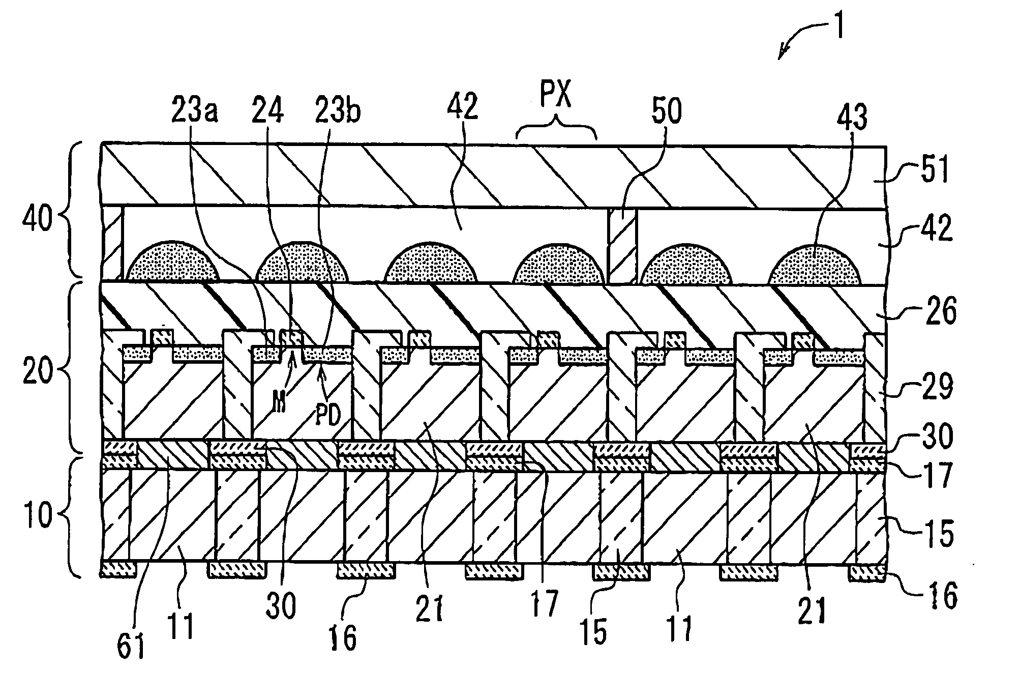
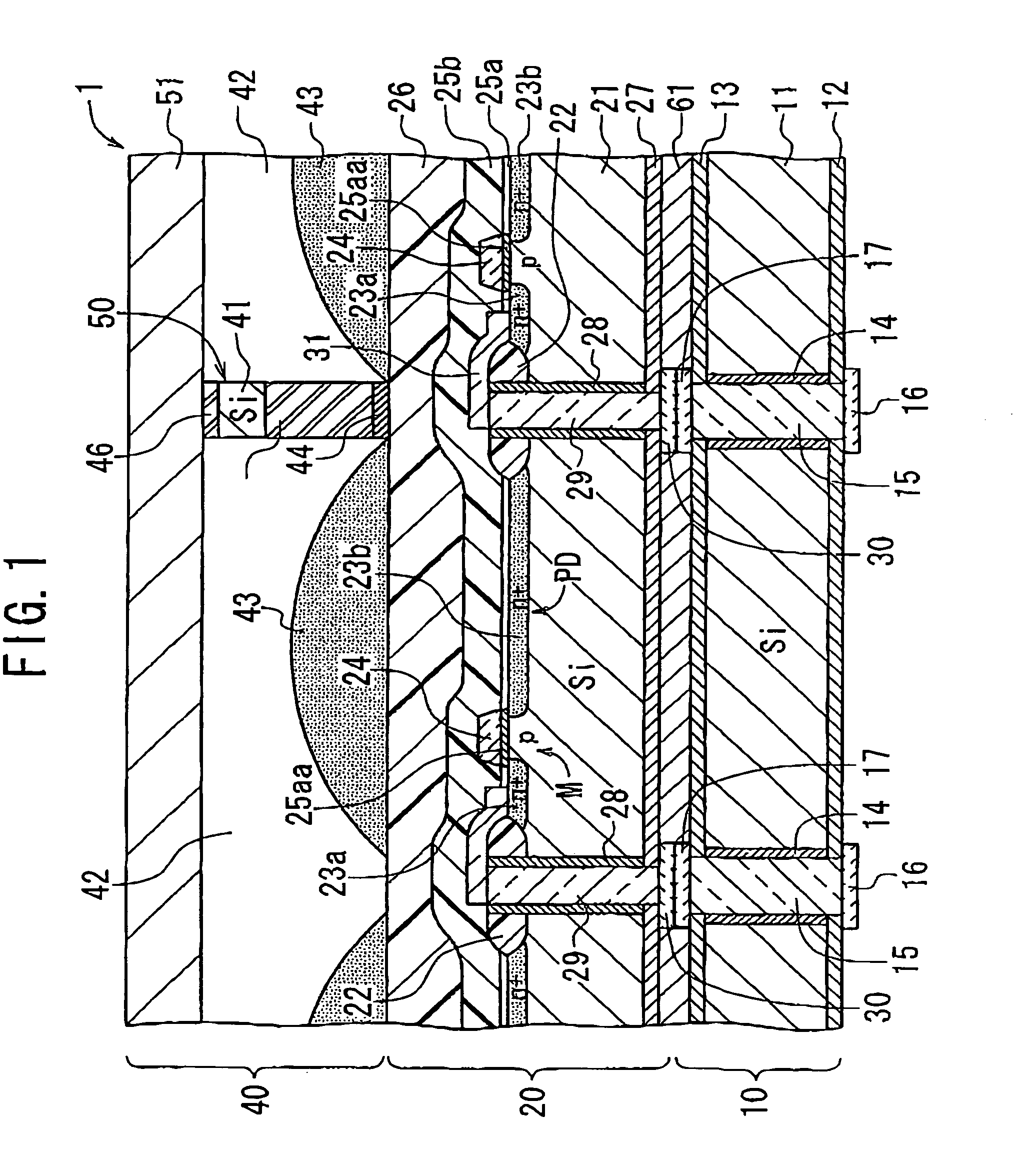
[0127]FIG. 2 is a partial, cross-sectional view showing the configuration of a main part of a solid-stage image sensor 1 according to a first embodiment of the invention, and FIG. 1 is a partial, enlarged cross-sectional view of the sensor 1.
[0128] As shown in FIGS. 1 and 2, the solid-state image sensor 1 has a three-layer structure comprising an output layer 10, a light-receiving element layer 20, and a light-introducing layer 40. The sensor 1 has pixel regions PX arranged in a matrix array. The sensor 1 picks up an image and converts it to electric signals in all the pixel regions PX and thereafter, outputs the electric signals. Each pixel region PX has a rectangular plan shape in this embodiment; however, needless to say, it may have any other plan shape, such as circular or hexagonal one.
[0129] The light-introducing layer 40 picks up light from an image located outside the image sensor 1 (i.e., an external image) and sends the l...
second embodiment
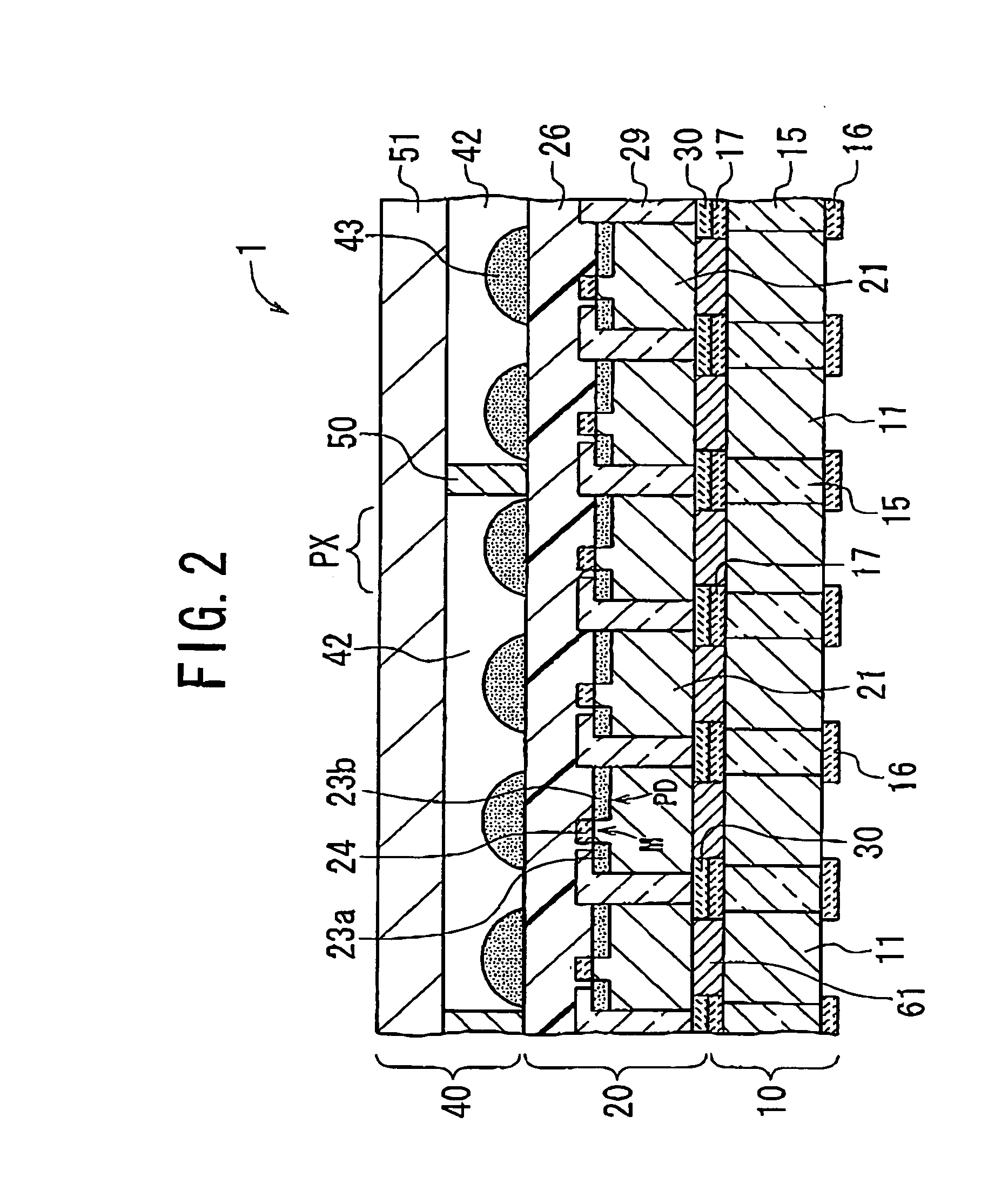
[0201]FIG. 14 shows the configuration of a solid-state image sensor 1A according to a second embodiment of the invention.
[0202] The image sensor 1A corresponds to one obtained by shifting the switching MOS transistors M to the output layer 10 from the light-receiving element layer 20 in the image sensor 1 according to the first embodiment. The other configuration of the sensor 1A is the same as the sensor 1. Therefore, explanation about the same configuration is omitted by attaching the same reference symbols as those used in the sensor 1 of the first embodiment to corresponding elements in FIG. 14.
[0203] As shown in FIG. 14, the image sensor 1A has a three-layer structure like the image sensor 1 of the first embodiment.
[0204] In the light-receiving element layer 20′, a n+-type diffusion region 23 is formed in each of the element-formation regions formed in the p-type single-crystalSi substrate 21. That is, only a photodiode PD is formed in each element-formation region. The sen...
third embodiment
[0217]FIG. 15 shows the configuration of a solid-state image sensor 1B according to a third embodiment of the invention.
[0218] The sensor 1B corresponds to one obtained by providing light-receiving MOS transistors (i.e., phototransistors) M′ in the light-receiving element layer 20″ instead of the photodiodes PD in the solid-state image sensor 1A according to the second embodiment of FIG. 14. The other configuration of the sensor 1B is the same as the sensor 1A. The structure of the transistors M′ of the layer 20″ is substantially the same as that of the transistors M of the output layer 10″.
[0219] As shown in FIG. 15, the image sensor 1B has a three-layer structure as well. In the light-receiving element layer 20″, a pair of source / drain regions 23a and 23b is formed in each of the element-formation regions formed on the lower side of the single-crystalSi substrate 21. The sensor 1B is different from the sensors 1 and 1A according to the second and third embodiments at this point...
PUM
Abstract
A solid-state image sensor has a chip-size package, which can be easily fabricated. The element-formation regions are formed in the semiconductor substrate (21) of the light-receiving element layer (20) corresponding to the pixel regions. The semiconductor light-receiving elements (PD) are formed in the respective element-formation regions and covered with the light-transmissive insulator films (25a), (25b) and (26). The light-introducing layer (40), which includes the light-introducing cavity (42) and the quartz cap (51) for closing the cavity, is formed on the film (26). The microlenses (43) are incorporated into the cavity (42). The electric output signals of the semiconductor light-receiving elements (PD) are taken out to the bottom of the substrate (21) by way of the buried interconnections of the substrate (21) and then, derived to the outside of the image sensor by way of the output layer (10) or the interposer (10A).
Description
TECHNICAL FIELD [0001] The present invention relates to a solid-state image sensor and a method of fabricating the same and more particularly, to a solid-state Image sensor having microlenses arranged regularly and a method of fabricating the sensor. BACKGROUND ART [0002] Conventionally, solid-state image sensors have been frequently used in various solid-state image pickup apparatuses for capturing exterior image information and converting it to electric signals, such as digital cameras and facsimiles. Solid-state image sensors of this type are roughly divided into the so-called “line sensor” having pixel regions aligned in one direction (i.e., one-dimensionally) and the so-called “area-sensors” having pixel regions arranged in an area (i.e., two-dimensionally). Conventional solid-state image sensors of this type generally have the following configuration. [0003] Specifically, semiconductor light-receiving elements are regularly arranged corresponding to pixel regions. Light from a...
Claims
Application Information
Patent Timeline
Application Date:The date an application was filed.
Publication Date:The date a patent or application was officially published.
First Publication Date:The earliest publication date of a patent with the same application number.
Issue Date:Publication date of the patent grant document.
PCT Entry Date:The Entry date of PCT National Phase.
Estimated Expiry Date:The statutory expiry date of a patent right according to the Patent Law, and it is the longest term of protection that the patent right can achieve without the termination of the patent right due to other reasons(Term extension factor has been taken into account ).
Invalid Date:Actual expiry date is based on effective date or publication date of legal transaction data of invalid patent.

