Mos semiconductor device

a semiconductor device and semiconductor technology, applied in the direction of semiconductor devices, electrical appliances, transistors, etc., can solve the problems of difficult to obtain a sufficiently high mobility, unsuitable for the case, and inability to achieve the first conventional method

Inactive Publication Date: 2005-02-10
RENESAS ELECTRONICS CORP
View PDF15 Cites 36 Cited by
  • Summary
  • Abstract
  • Description
  • Claims
  • Application Information

AI Technical Summary

Benefits of technology

[0029]FIG. 14 is a schematic view of a p-channel MOS field effect transistor with a short source/drain length for investigation on a

Problems solved by technology

The first conventional method has problems for how to keep a surface planarity of Si layer grown over the relaxed layer as well as how to reduce defects in the related layer or the strained Si layer.
The first conventional method is not practically realizable.
In accordance with the first conventional method, a strain of at most 0.3

Method used


Image

  • Mos semiconductor device
  • Mos semiconductor device
  • Mos semiconductor device

Examples


first embodiment

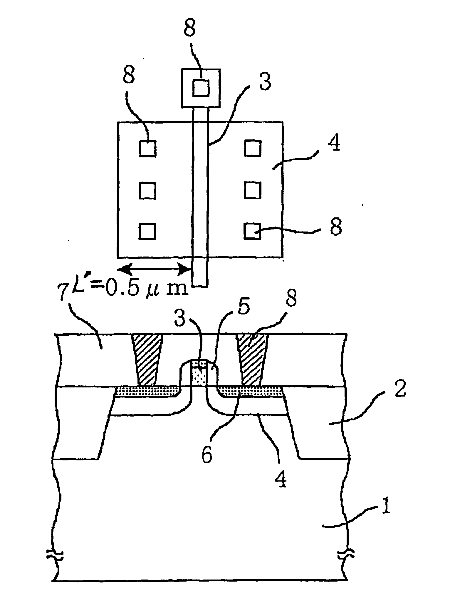
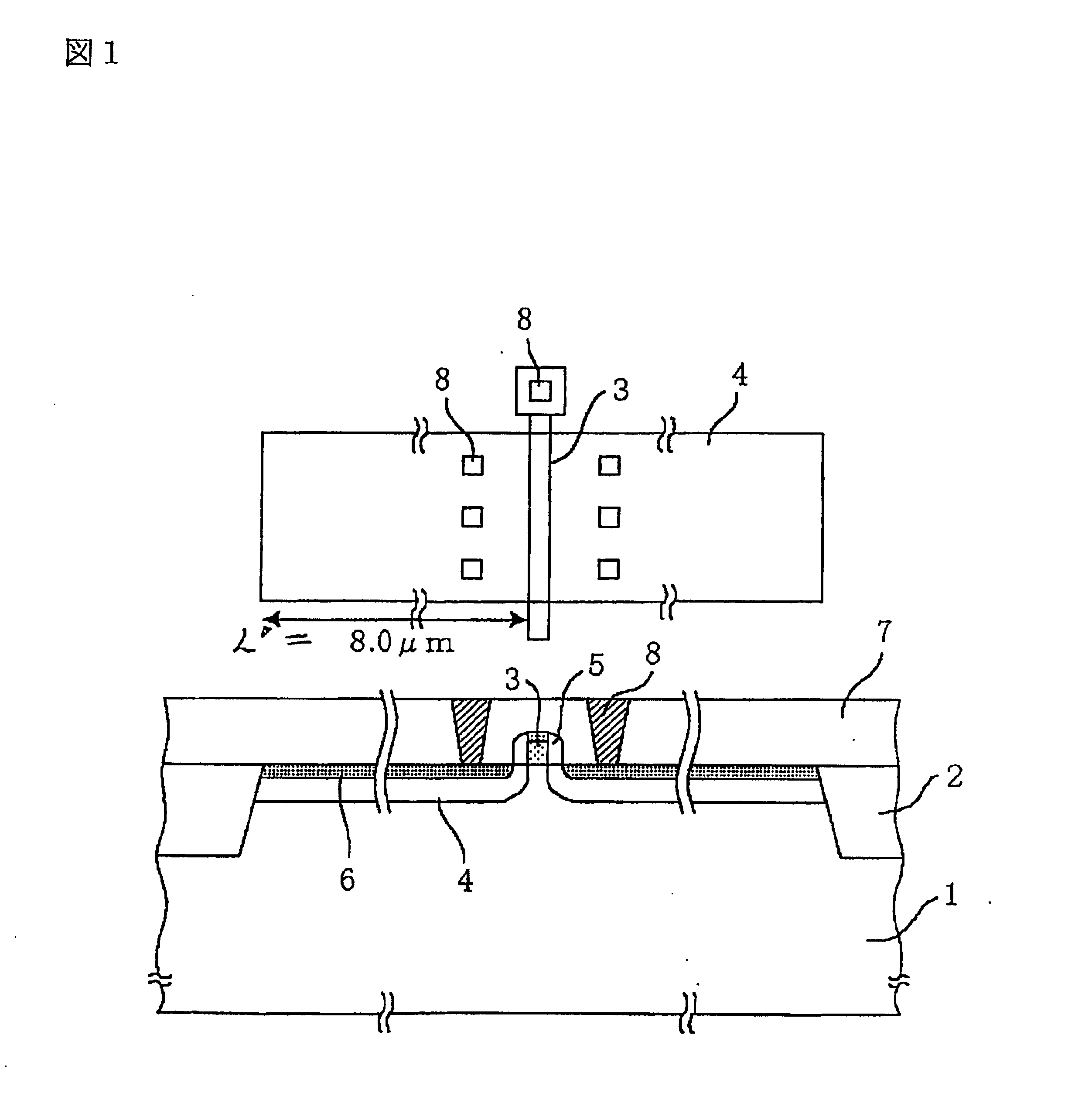
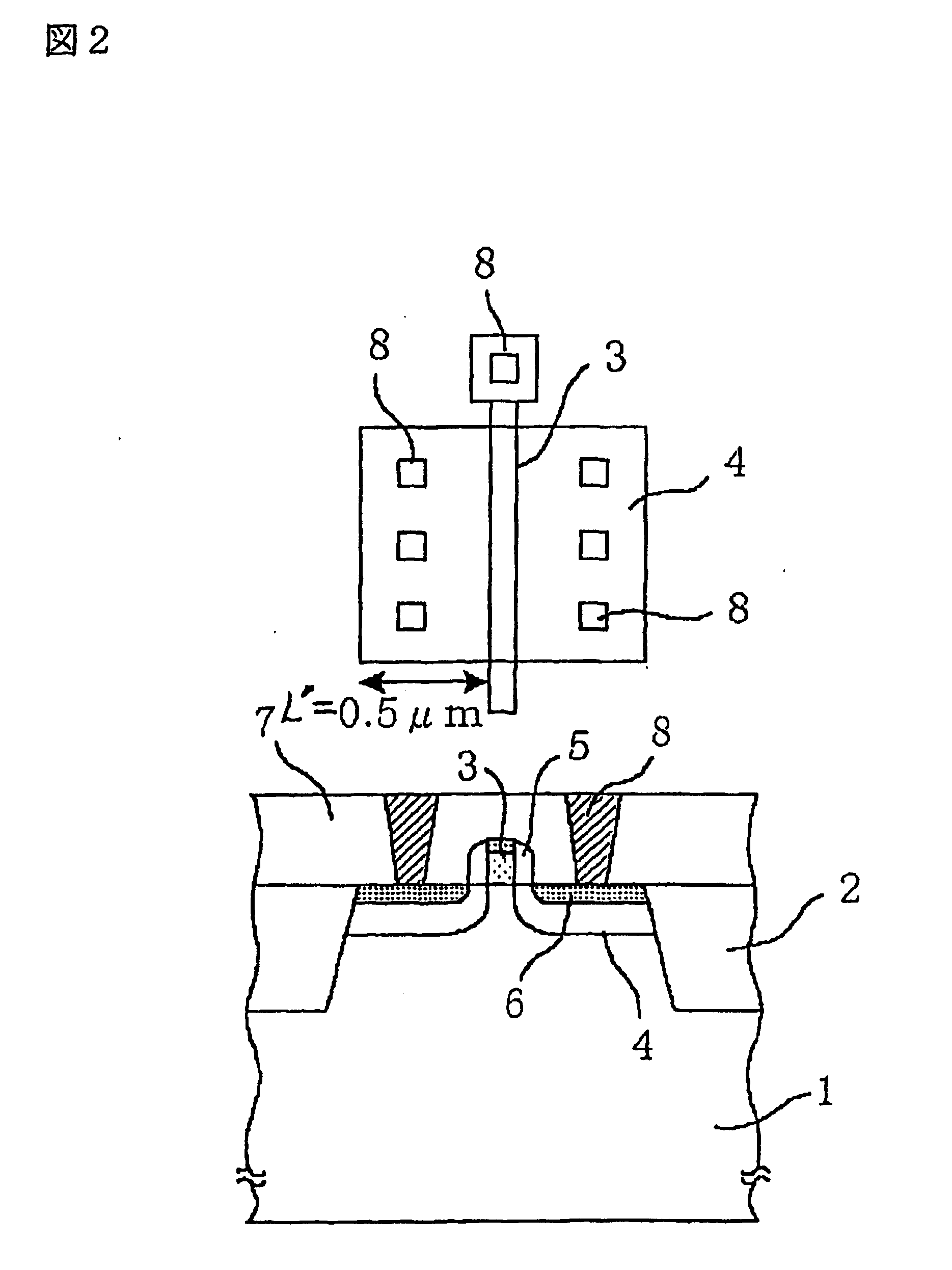
[0031] The present inventors investigated a channel region with a strain introduced by an STI (shallow trench isolation)-type device isolation region as well as an influence of this strain to an ON-current. For this purpose, two p-channel MOS field effect transistors were prepared and measured in lattice strain of channel region and in ON-current, wherein the two p-channel MOS field effect transistors are different in a distance L′ between the device isolation film and the channel or source / drain length as shown in FIGS. 1 and 2. FIG. 1 shows a first p-channel MOS field effect transistor with a long source / drain length. FIG. 2 shows a second p-channel MOS field effect transistor with a short source / drain length.

[0032] As shown in FIG. 1, the first p-channel MOS field effect transistor has the following structure. An active region is isolated by an STI (shallow trench isolation)-type device isolation film 2 over a silicon substrate 1. A gate insulation film (not illustrated) is form...

second embodiment

[0045] In accordance with the above-described first embodiment, the p-channel MOS field effect transistor is improved in ON-current by applying the compressive strain in the channel direction to the p-channel MOS field effect transistor. Application of the compressive strain in the channel direction to the n-channel MOS field effect transistor causes decrease of the ON-current. It is necessary for the n-channel MOS field effect transistor to introduce a tensile strain in the channel direction into the n-channel MOS field effect transistor to improve the ON-current thereof.

[0046] In accordance with this second embodiment, a silicon nitride film is inserted into the STI-type device isolation film to introduce the tensile strain in the channel direction into the n-channel MOS field effect transistor to improve the ON-current thereof. FIG. 6 shows schematically the section of the device isolation film with the inserted silicon nitride film. The STI-type device isolation comprises a sil...

third embodiment

[0054]FIG. 9 is fragmentary plan and sectional views showing a CMOS structure in accordance with the third embodiment of the present invention. in FIG. 9, the same reference numbers are allocated to the same parts as shown in FIGS. 1 and 2. Duplicate descriptions will be omitted. In the third embodiment shown in FIG. 9, a p-well 1a and an n-well 1b are formed over a silicon substrate 1. An n-channel MOS field effect transistor and a p-channel MOS field effect transistor are formed over those wells. As shown in the same drawing, in accordance with this embodiment, the CMOS structure comprises the n-channel MOS field effect transistor with a long source / drain length L′ and the p-channel MOS field effect transistor with a short source / drain length L′. If the source / drain length L′ is short, then the hole mobility is increased, while the electron mobility is decreased. If both the n-channel and p-channel MOS field effect transistors have short source / drain length, then the n-channel MOS...


PUM


Abstract

While using conventional manufacturing processes, it is intended to apply a compressive strain in the channel direction to the p-channel MOS field effect transistor and also apply a tensile strain in the channel direction to the n-channel MOS field effect transistor for increasing both MOS currents. In the MOS semiconductor device isolated by a trench device isolation region, the p-channel MOS field effect transistor is designed so that a length of a source/drain region in the channel direction is not more than 1 micrometer, and the gate length is not more than 0.2 micrometers. The n-channel MOS field effect transistor is designed so that a face of the source/drain region in parallel to the gate width direction is adjacent to the device isolation film with the inserted silicon nitride film, and a face of the source/drain region parallel to the gate length direction is adjacent to the device isolation film comprising the silicon oxide film only.

Description

TECHNICAL FIELD [0001] The present invention relates to a MOS semiconductor device having a MOS field effect transistor, and more particularly to a MOS semiconductor device including at least one of a p-channel MOS field effect transistor and an n-channel MOS field effect transistor which are improved in ON-current. BACKGROUND ART [0002] Improvements in performances of MOS transistors and CMOS have been made by shrinkage or scaling down thereof, for example, shortening a channel length and a reduction in thickness of a gate insulating film. A reduction in thickness of the gate insulating film and a minimum size or dimension for process have become closer to the limitations. A further improvement in performance can not depend upon the limited shrinkage or scaling down of the device, but should depend upon any other measures than the shrinkage or scaling down of the device. [0003] One of the improvements in performance of the device is a technique of applying a stress to a channel reg...

Claims


Application Information

Patent Timeline
IPC IPC(8): H01L21/76H01L21/336H01L21/8238H01L27/08H01L27/088H01L27/092H01L29/78
CPCH01L21/823807H01L21/823878H01L2924/0002H01L29/7842H01L2924/00H01L29/7846H01L29/0692
Inventor TODA, AKIOONO, HARUIHIKO
Owner RENESAS ELECTRONICS CORP
Why Eureka
Try Eureka