Methods of forming hemispherical grained silicon on a template on a semiconductor work object

Inactive Publication Date: 2005-02-10
MICRON TECH INC
View PDF28 Cites 16 Cited by
  • Summary
  • Abstract
  • Description
  • Claims
  • Application Information

AI Technical Summary

Benefits of technology

[0017] Passivating the surface of the wafer to inhibit reforma

Problems solved by technology

As described in the aforementioned patents, the formation of a native oxide on a wafer's surface during wafer transfer steps causes significant problems in forming HSG structures on a wafer.
If the oxide layer is not removed or inadequately removed, it can impede the seeding step of the seeding/annealing process in HSG formation.
A persisting problem in HSG formation process is that existing process steps do not adequately etch the undesired oxide materials from the wafer.
Poor, irregularly shaped HSG formations result if the HSG process is not conducted on clean, properly prepped wafers.
There are further problems as well.
Existing techniques do not adequately passivate the wafer surface after etching.
Another etch-related problem is that conventional etching techniques do not have acceptable selectivity ratios for the different materials present during HSG formation.
Conventional cleaning and etching techniques may also leave the wafer's surface in poor condition for HSG seeding and annealing s

Method used


Image

  • Methods of forming hemispherical grained silicon on a template on a semiconductor work object
  • Methods of forming hemispherical grained silicon on a template on a semiconductor work object
  • Methods of forming hemispherical grained silicon on a template on a semiconductor work object

Examples


Example

[0038] The present invention provides a novel method for treating a semiconductor work object so that it is suitable for use in HSG process steps. As used herein, “work object” means wafers (production, dummy, or pmon), die and packaged parts, incorporating, in whole or part, silicon substrates, and other known or discovered semiconductor materials, components, and assemblies, including, for example, silicon-on-insulator (SOI), silicon-on-sapphire (SOS), thin film transistor (TFT) materials, or germanium, periodic group III-IV materials, II-VI materials, hetero-materials (II, III, V, VI), and conductive glasses.

[0039] It will be apparent to persons of skill in the art that the present invention is not necessarily limited to any particular kind of work object. However, to illustrate the principles of the present invention, the following discussion, unless otherwise noted, will be in terms of a silicon-based wafer as the work object.

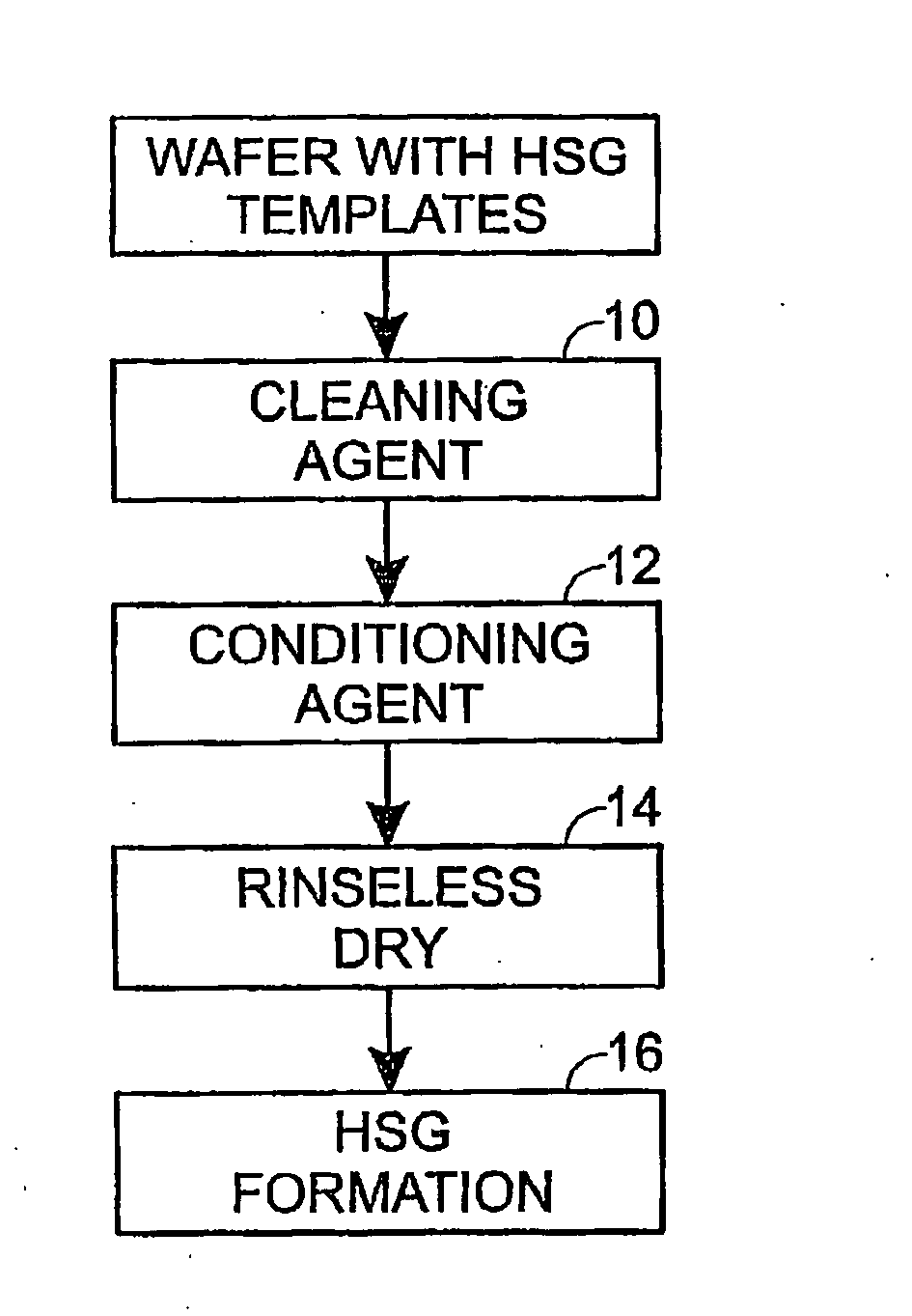
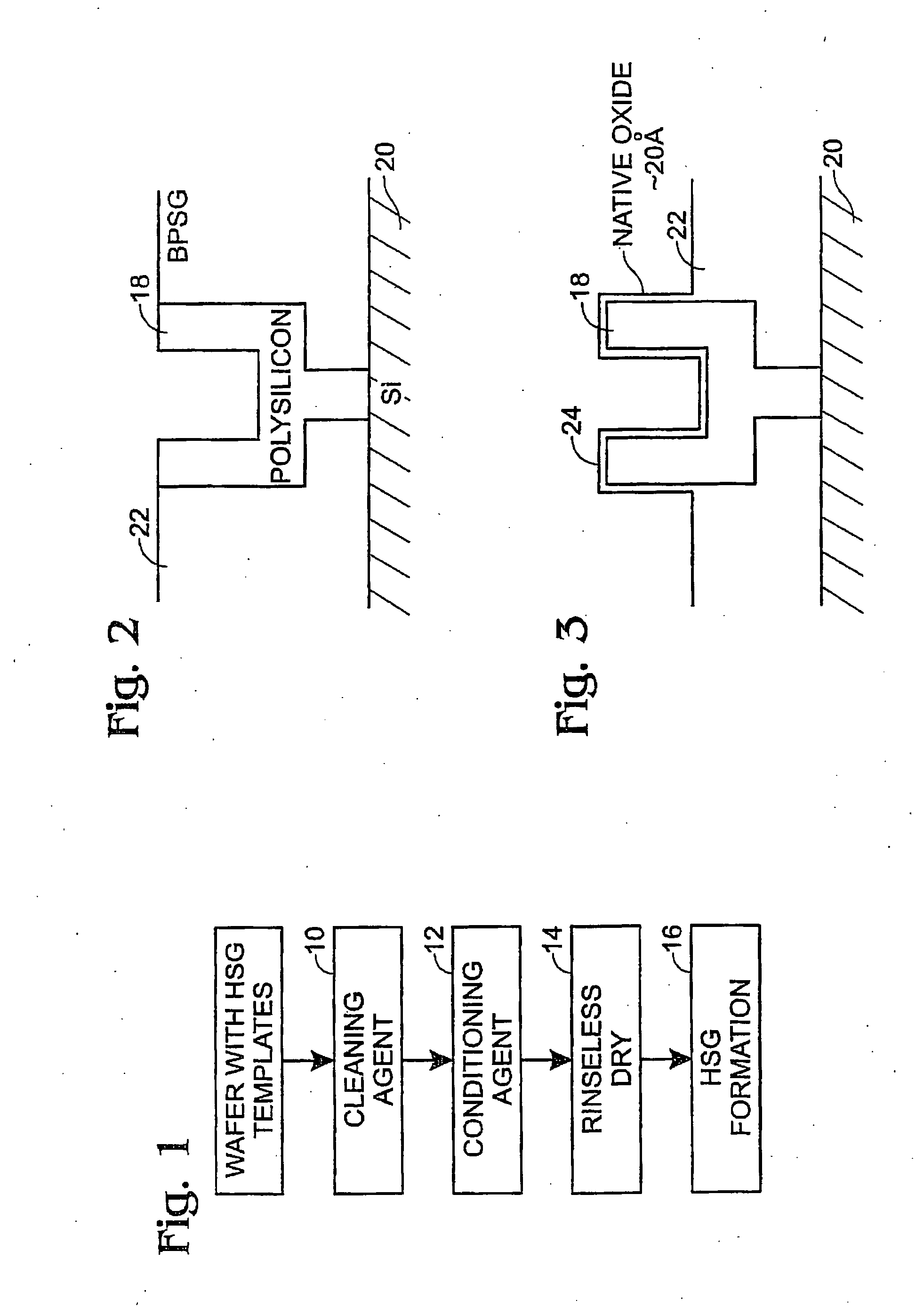
[0040]FIG. 1 is a flow chart of steps 10-16 that d...


PUM


Abstract

The present invention provides a method of preparing a surface of a silicon wafer for formation of HSG structures. The method contemplates providing a wafer having at least one HSG template comprising polysilicon formed in BPSG, the HSG template being covered by silicon dioxide. The wafer is treated with a cleaning agent to clean the surface of the wafer. Next, the wafer is treated with a conditioning agent. The conditioning agent removes native oxide from the HSG template without excessively etching structural BPSG. Preferably, the conditioning agent also removes a thin layer of polysilicon on the HSG template. The wafer is then transferred to a process chamber for HSG formation.

Description

[0001] This invention claims the benefit of co-pending U.S. application Ser. No. 10 / 174,696 entitled “Methods Of Forming Hemispherical Grained Silicon On A Template On A Semiconductor Work Object”, filed Jun. 18, 2002 which is a divisional of U.S. application Ser. No. 09 / 303,385, entitled “Method Of Forming Hemispherical Grained Silicon On A Template On A Semiconductor Work Object”, filed May 1, 1999, the entire disclosures of which are hereby incorporated by reference as if set forth in their entireties for all purposes.BACKGROUND OF THE INVENTION [0002] The present invention relates to a method of cleaning and conditioning a semiconductor work object, such as a silicon wafer, so that subsequent process steps produce desired results. More particularly, the present invention provides a method of cleaning and etching a wafer so that deposition of amorphous silicon (“a-Si”) on the wafer produces good formations of Hemispherical Grained Silicon (“HSG”). [0003] HSG formations enhance th...

Claims


Application Information

Patent Timeline
IPC IPC(8): H01L21/02
CPCH01L28/90H01L28/84
Inventor CHEN, GUOQINGPAN, JAMES
Owner MICRON TECH INC
Why Eureka
Try Eureka