Three demensional dynamicaly shielded high-q BEOL metallization

Inactive Publication Date: 2005-02-17
IBM CORP
View PDF11 Cites 10 Cited by
  • Summary
  • Abstract
  • Description
  • Claims
  • Application Information

AI Technical Summary

Benefits of technology

[0004] Accordingly, it is a primary object of the present invention to provide three dimensional, dynamically shielded, high Q BEOL metal elements. Conductive, three dimensional shielding structures for BEOL elements reduce or eliminate, parasitic capacitive coupling between the BEOL element and the conductive substrat

Problems solved by technology

Prior art implementations for BEOL inductor elements have utilized a buffered drive of adjacent spiral inductive elements to achieve a higher quality factor

Method used


Image

  • Three demensional dynamicaly shielded high-q BEOL metallization
  • Three demensional dynamicaly shielded high-q BEOL metallization

Examples


Embodiment Construction

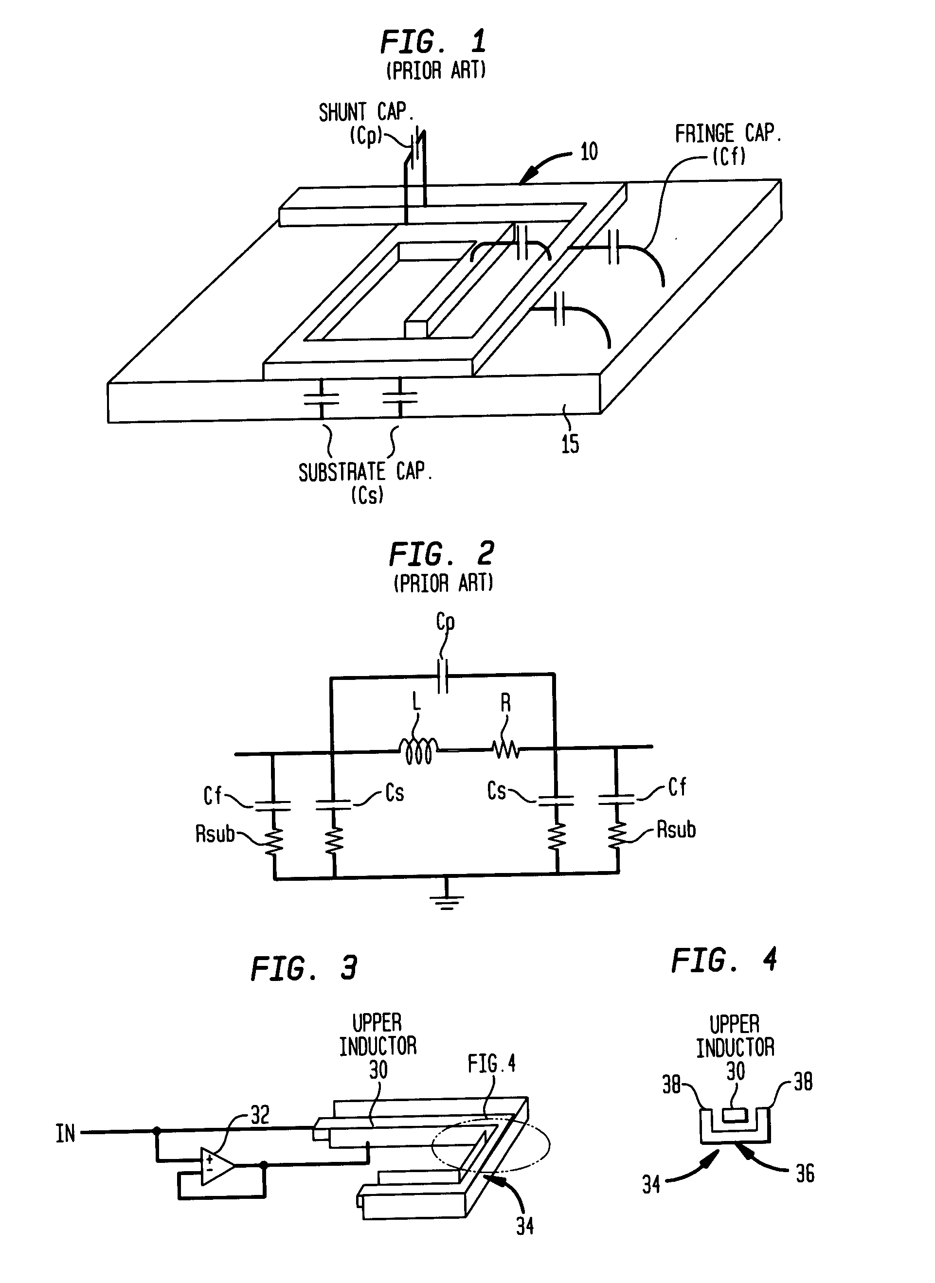
[0013]FIG. 1 illustrates a conventional prior art spiral type of inductor element realized in the BEOL (Back End Of Line) processing of monolithic integrated circuits. Such conventional prior art spiral inductor elements suffer from excessive power losses due to: 1) parasitic substrate capacitive coupling Cs between the inductor 10 and the conductive substrate 15; 2) parasitic fringe capacitance coupling Cf between the inductor 10 and the conductive substrate 15; and 3) parasitic shunt capacitance coupling Cp between different adjacent shunt sections of the inductor 10.

[0014] These excessive power losses make it difficult to achieve System On Chip (SOC) applications due to the relatively low Q of the integrated passive inductors.

[0015]FIG. 2 illustrates an equivalent circuit for a conventional prior art spiral type of inductor element. The inductor is illustrated as having an equivalent inductive component L and a resistive component R, with a parasitic substrate capacitive coupli...


PUM


Abstract

Three dimensional dynamically shielded high quality factor (Q) BEOL metal elements, such as inductor elements, are disclosed. Three dimensional shielding structures for the BEOL elements reduce or eliminate parasitic substrate capacitive coupling between the BEOL element and the conductive substrate, and parasitic shunt capacitance coupling between different adjacent shunt sections of the BEOL element. The reduction or elimination of the parasitic capacitive components provides high Q BEOL metal elements such as inductor elements. The three dimensional shield structure includes a lower shield surface having a width greater than the width of the BEOL element, and opposed side shield surfaces which extend upwardly from opposite side edges of the lower shield surface, such that the three dimensional shield element forms a U shaped shield around the BEOL element. The three dimensional shield element is dynamically driven to the same electrical potential as the BEOL element, to substantially eliminate the metal element's parasitic capacitances.

Description

BACKGROUND OF INVENTION [0001] The present invention relates generally to the realization of RF passive elements and interconnect metallization with very low parasitic capacitance to an underlying conductive substrate and adjacent metallization through the use of conductive, three dimensional, dynamic shielding. More particularly, the subject invention pertains to three dimensional, dynamically shielded metal elements such as inductors, MIM (metal-insulator-metal) capacitors, resistors, wirebond pads, and stable bias lines constructed in the interconnect metallization layers (Back End Of Line, BEOL) of a monolithic, integrated circuit. This three dimensional shielding of the BEOL elements (inductors, capacitors, resistors, etc.) reduces or eliminates the parasitic capacitive coupling between the element and the conductive substrate. Additionally, parasitic fringe capacitance coupling between the specific BEOL element and adjacent areas of metallization is reduced or eliminated, gene...

Claims


Application Information

Patent Timeline
IPC IPC(8): H01F17/00H01L23/522H05K1/02H05K1/16H05K9/00
CPCH01F2017/008H01L23/5222H01L23/5227H01L2924/3011H05K1/0219H01L2924/0002H05K1/165H01L2924/00
Inventor GROVES, ROBERT A.PARK, JAE-EUN
Owner IBM CORP
Why Eureka
Try Eureka