Thin film semiconductor element and method of manufacturing the same

a technology of thin film and semiconductor elements, applied in the direction of semiconductor devices, electrical equipment, radio frequency control devices, etc., can solve the problems of lowering the reliability of semiconductor elements, and achieve the effect of preventing the generation of leakage current and improving etching characteristics

Active Publication Date: 2005-02-17
SHENZHEN CHINA STAR OPTOELECTRONICS TECH CO LTD
View PDF3 Cites 24 Cited by
  • Summary
  • Abstract
  • Description
  • Claims
  • Application Information

AI Technical Summary

Benefits of technology

[0043] According to the invention, in the process of forming the source and drain electrodes using a dry etching method, the first lowest-layer metal is removed to surround the upper layer metal which is located on the upper side of the first lowest-layer metal. Furthermore, since the first lowest-layer metal is formed to be thicker, with the progress of the dry etching, the first

Problems solved by technology

Therefore, if the thickness of the Al layer in the source and drain electrode material SD is larger, both Al and Ti are left as residues on

Method used


Image

  • Thin film semiconductor element and method of manufacturing the same
  • Thin film semiconductor element and method of manufacturing the same
  • Thin film semiconductor element and method of manufacturing the same

Examples


Embodiment Construction

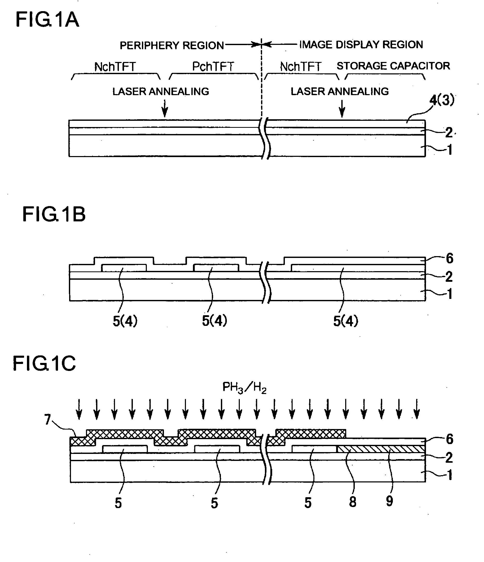
[0055] An embodiment of the invention will now be explained referring to FIGS. 1 to 7.

[0056] In the embodiment, a TFT array substrate constituting an active matrix liquid crystal display device is explained as an example of a thin film semiconductor element of the present invention. Further, a manufacturing process of a low-temperature polysilicon TFT is cited as an example of a TFT manufacturing process.

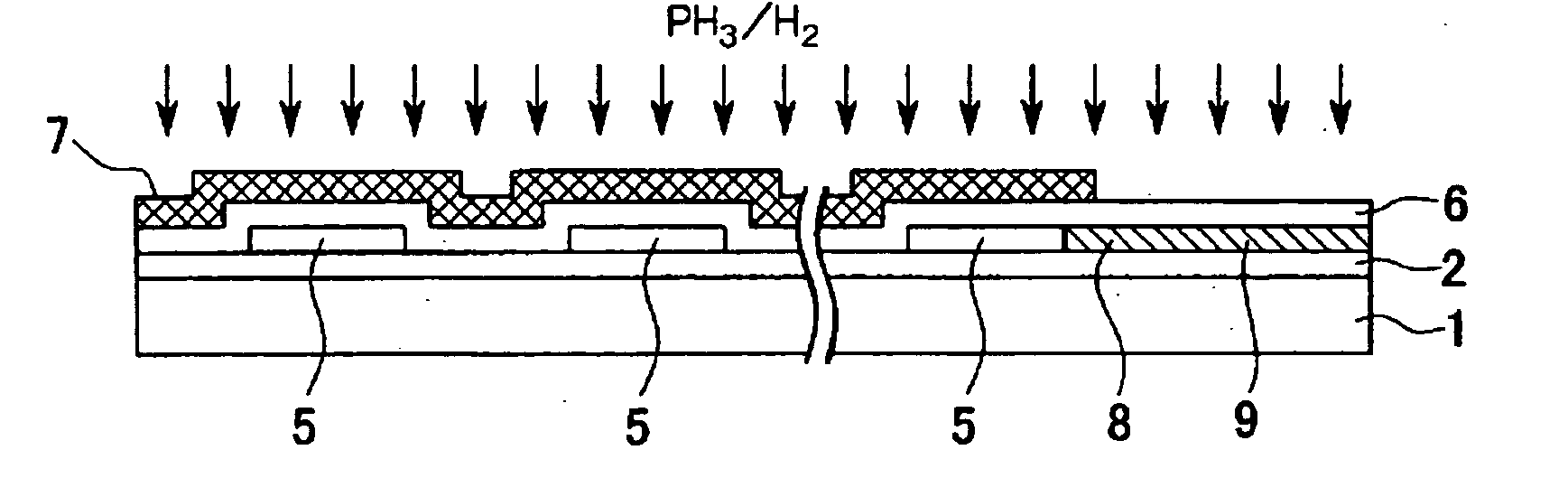
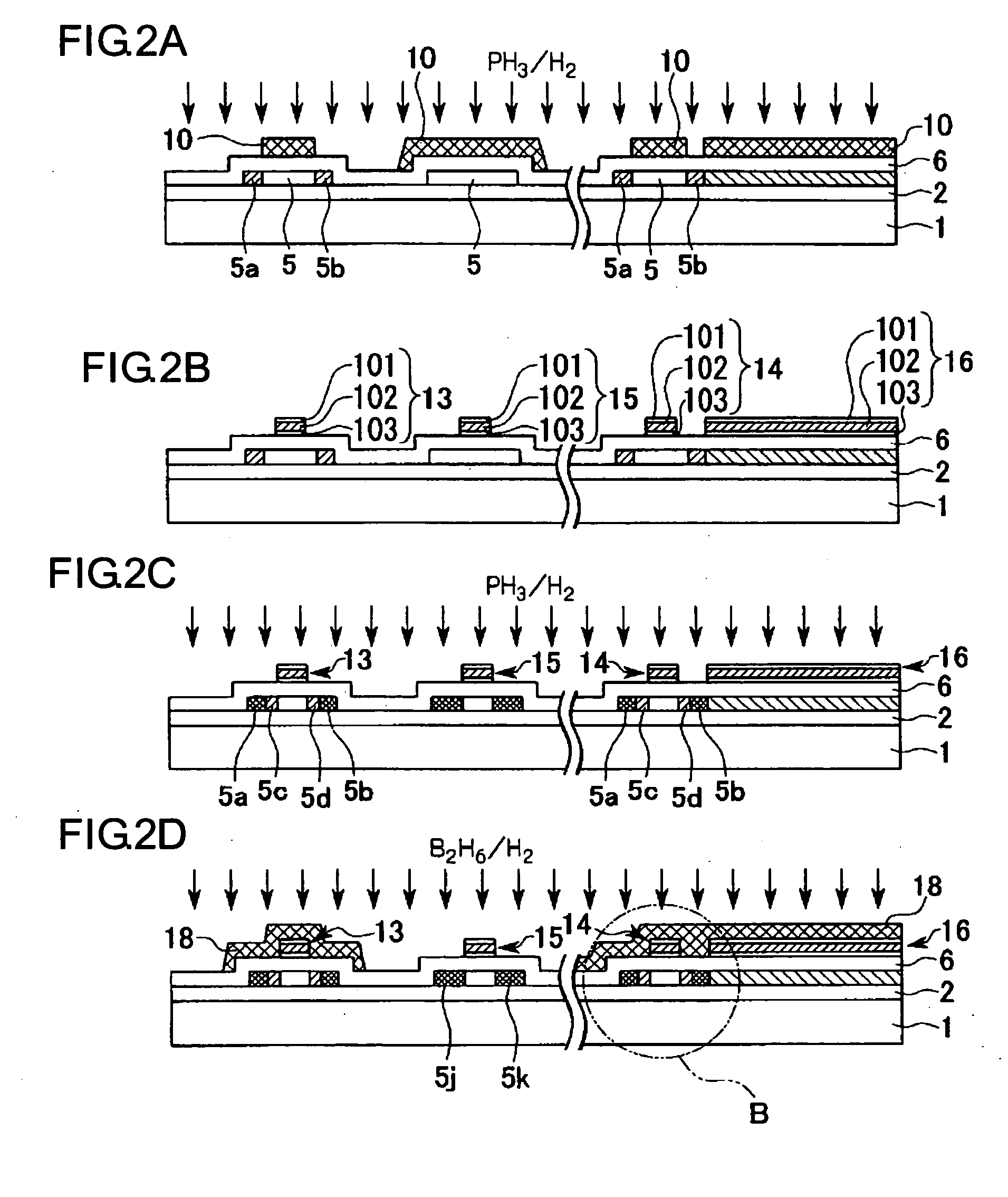
[0057] FIGS. 1 to 4 are cross-sectional views to illustrate processes of manufacturing a thin film semiconductor of the present embodiment in order. FIG. 5 is a diagram illustrating the film thickness relationship of the main part in the thin film semiconductor element. FIG. 6 is a plan view of a TFT array substrate on which various components are formed, as seen from the side of a counter substrate. FIG. 7 is a cross-sectional view taken along the line H-H′ of FIG. 6.

[0058] Further, in FIGS. 1 to 7, different scales are applied to each layer and element to understandably illustr...


PUM


Abstract

The invention provides a thin film semiconductor element and a method of manufacturing the same to achieve lowering the resistance of gate electrodes, lowering the capacitance of source electrodes, and enhancing etching characteristics. The thin film semiconductor element can include a semiconductor film provided on a substrate, source and drain electrodes connected to the semiconductor film, and a gate electrode provided on the semiconductor film with an insulating film interposed therebetween. The film thickness of the source and drain electrodes can be smaller than the film thickness of the gate electrode.

Description

BACKGROUND OF THE INVENTION [0001] 1. Field of Invention [0002] The present invention relates to a thin film semiconductor element and a method of manufacturing the same [0003] 2. Description of Related Art [0004] In active matrix substrates constituting electro-optical devices, such as liquid crystal display devices, thin film transistors (TFTs) have been used as switching elements. According to recent trend, patterning wiring lines finely for a TFT circuit accompanied with the narrow pixel pitch in a liquid crystal display device, or lowering TFT driving power accompanied with making the substrate large are required. [0005] From the point of view, it has been considered to adopt a low resistance metal as a material for wiring lines or electrodes, such as gate electrodes or source and drain electrodes, in the TFT circuit. Particularly, it has been suggested that an aluminum-based material is used as the low resistance metal. See, for example, Japanese Unexamined Patent Application ...

Claims


Application Information

Patent Timeline
IPC IPC(8): H01L21/28H01L21/336H01L21/77H01L21/8238H01L21/84H01L27/08H01L27/092H01L27/12H01L29/417H01L29/423H01L29/45H01L29/49H01L29/786
CPCH01L27/12H01L29/41733H01L27/124H01L29/458H01L29/4908H01L29/42384H01L27/1214
Inventor ONIZUKA, TATSUYA
Owner SHENZHEN CHINA STAR OPTOELECTRONICS TECH CO LTD
Why Eureka
Try Eureka