Distributed amplifier optical modulators

a technology of optical modulators and amplifiers, applied in the field of optical modulators, can solve the problems that low-speed devices are not suitable for high-speed ghz rate systems, and achieve the effects of reducing capacitance, improving modulating speed, and improving modulating speed

Active Publication Date: 2005-02-17
CISCO TECH INC
View PDF13 Cites 32 Cited by
  • Summary
  • Abstract
  • Description
  • Claims
  • Application Information

AI Technical Summary

Benefits of technology

[0007] High speed optical modulators can be made of k modulators connected in series disposed on one of a variety of semiconductor substrates or wafers. An electrical signal propagating in a microwave transmission line is tapped off of the transmission line at regular intervals and is amplified by k distributed amplifiers. Each of the outputs of the k distributed amplifiers is connected to a

Problems solved by technology

These large modulators are relatively low speed devices capable of modulation at rates in the tens

Method used


Image

  • Distributed amplifier optical modulators
  • Distributed amplifier optical modulators
  • Distributed amplifier optical modulators

Examples


Embodiment Construction

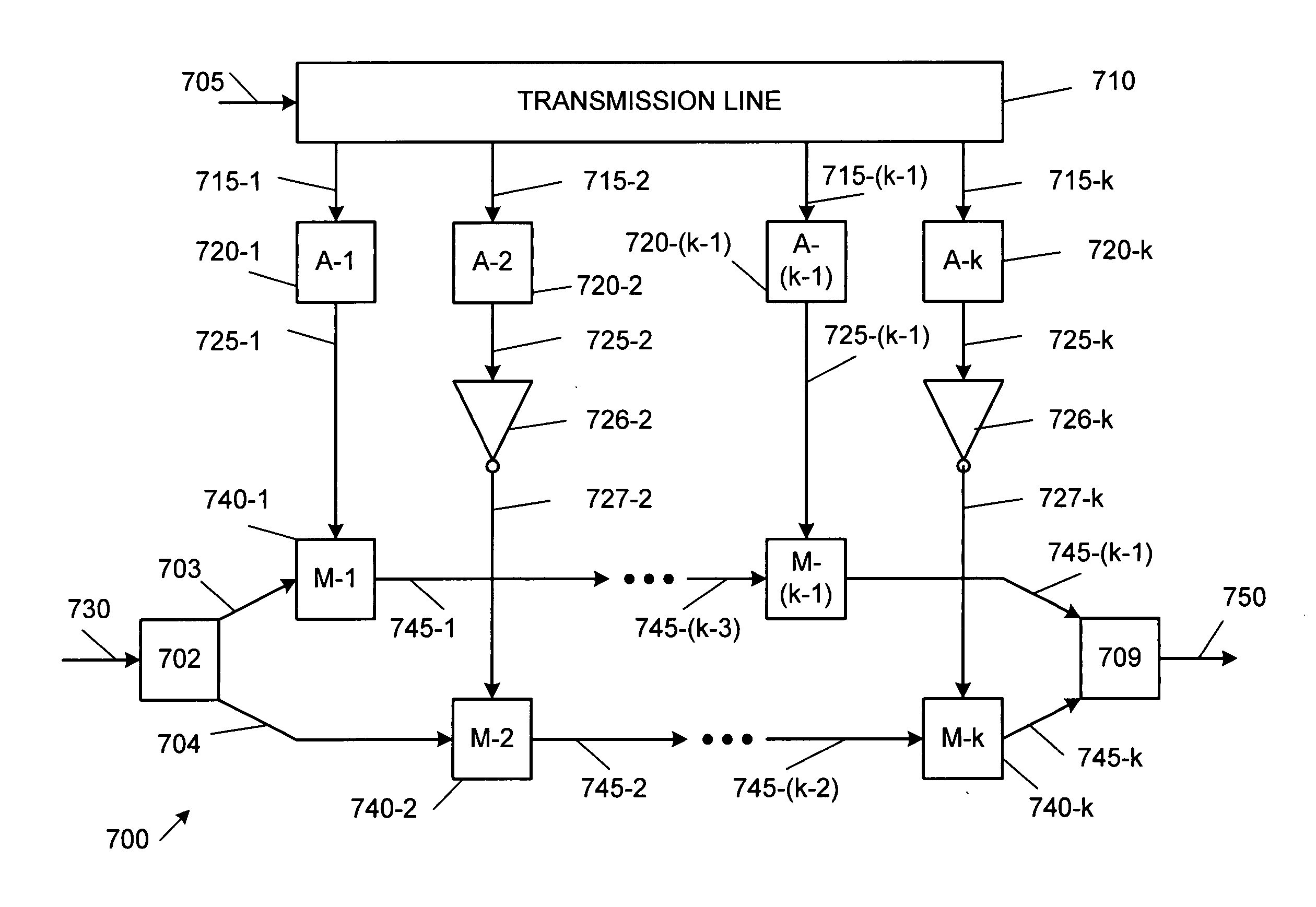
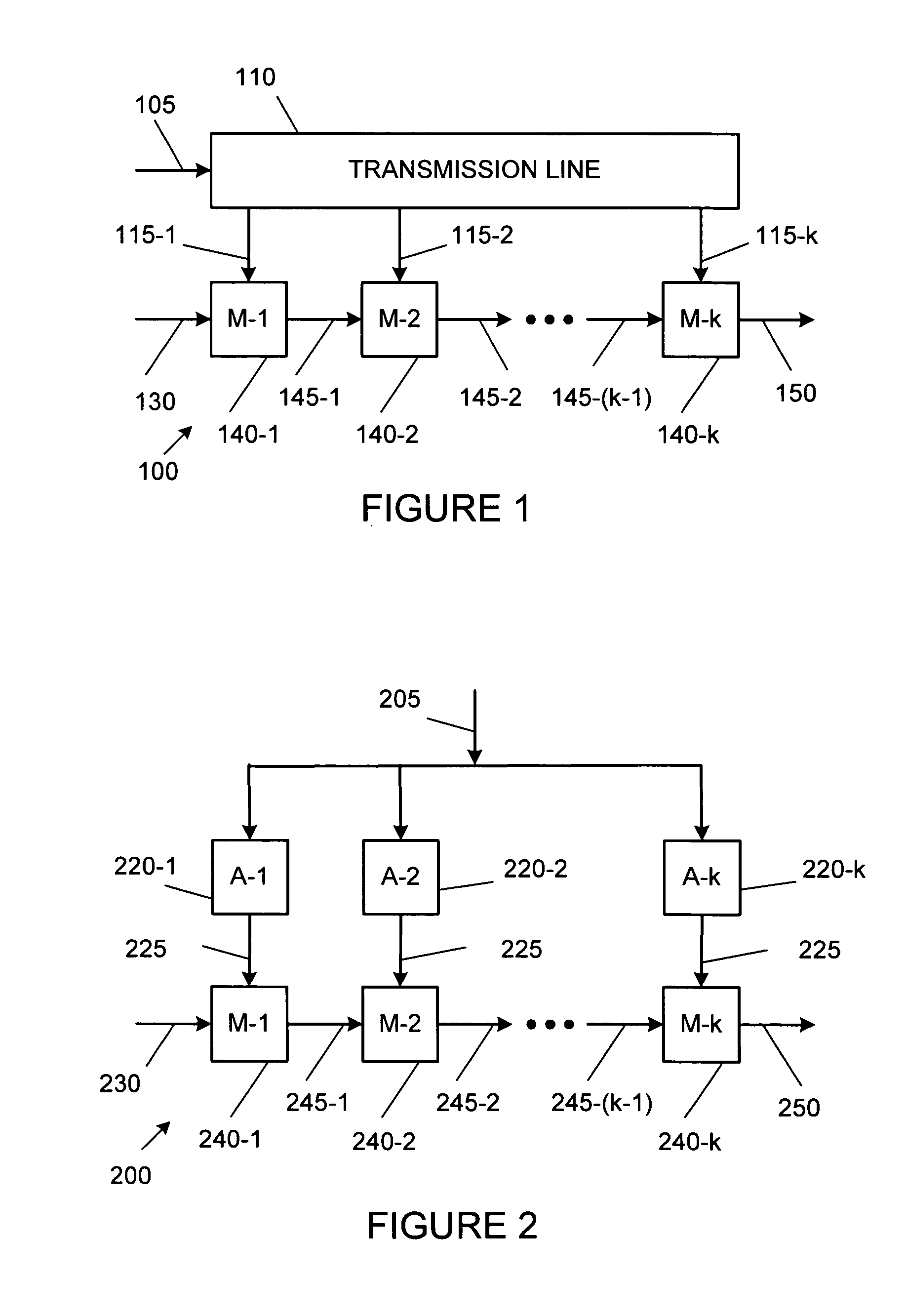
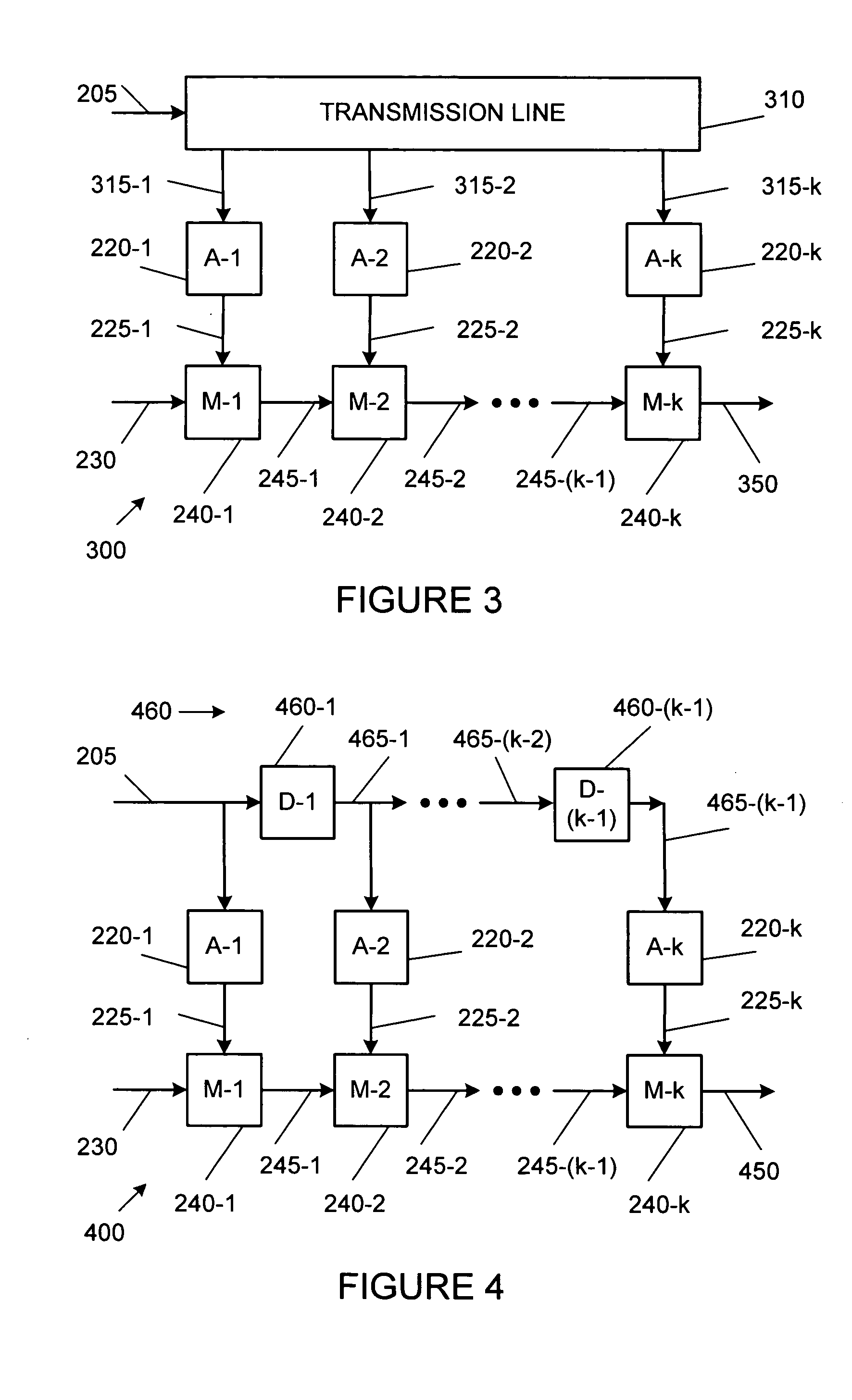
[0015]FIG. 1 is a block diagram of a prior art traveling wave (TW) integrated optical modulator. Traveling wave modulator 100 is made of transmission line (TL) 110 and series connected k modulating elements 140-1 to 140-k (M-1 to M-k). TL 110 receives modulating signal 105 at its input port and has k output ports 115-1 to 115-k. The output ports 115-1 to 115-k can be equally spaced apart along the length of TL 110, which would correspond to equal amounts of delay between the output ports. The distribution of ports along the length of TL 110 can follow some other distribution. Each of the outputs 115-j is delayed relative to the previous output 115-(j−1), depending on the length of the transmission line between any two adjacent output ports. Each of the k outputs is connected to the modulating input terminals of the respective k optical modulating elements 140-1 to 140-k connected in series.

[0016] Optical carrier 130 is connected to the carrier input of the first modulator 140-1. Th...


PUM


Abstract

High speed optical modulators can be made of k modulators connected in series disposed on one of a variety of semiconductor substrates. An electrical signal propagating in a microwave transmission line is tapped off of the transmission line at regular intervals and is amplified by k distributed amplifiers. Each of the outputs of the k distributed amplifiers is connected to a respective one of the k modulators. Distributed amplifier modulators can have much higher modulating speeds than a comparable lumped element modulator, due to the lower capacitance of each of the k modulators. Distributed amplifier modulators can have much higher modulating speeds than a comparable traveling wave modulator, due to the impedance matching provided by the distributed amplifiers.

Description

CROSS-REFERENCE TO RELATED APPLICATIONS [0001] This application claims priority from U.S. Provisional applications No. 60 / 495,402, No. 60 / 495,403 and No. 60 / 495,404 filed Aug. 15, 2003.FIELD OF THE INVENTION [0002] The present invention relates to optical modulators for use in optoelectronic integrated circuits. BACKGROUND OF THE INVENTION [0003] Optical fibers have been widely used for the propagation of optical signals, especially to provide high speed communications links. Optical links using fiber optics have many advantages compared to electrical links: large bandwidth, high noise immunity, reduced power dissipation and minimal crosstalk. Fiber optic communications links can operate with carrier frequencies in the THz range. In communications systems where optical fibers are used to transport optical communications signals, various optoelectronic devices are used to control, modify and process the optical signals. [0004] An integrated optical modulator is a key component of an ...

Claims


Application Information

Patent Timeline
IPC IPC(8): G02B6/12G02FG02F1/01G02F1/025G02F1/225H04B10/04
CPCG02B2006/12142G02B2006/12159G02F1/025G02F1/2255G02F1/2257G02F2201/127G02F1/0121G02F2201/20H01S5/0265H01S5/5027H04B10/5051H04B10/5053G02F2201/16
Inventor GUNN, LAWRENCE C. IIIKOUMANS, ROGERLI, BINGLI, GUO LIANGPINGUET, THIERRY J.
Owner CISCO TECH INC
Why Eureka
Try Eureka