

High-power infrared semiconductor diode light emitting device
- Summary
- Abstract
- Description
- Claims
- Application Information
AI Technical Summary
Benefits of technology
Problems solved by technology
Method used
Image

Examples
Embodiment Construction
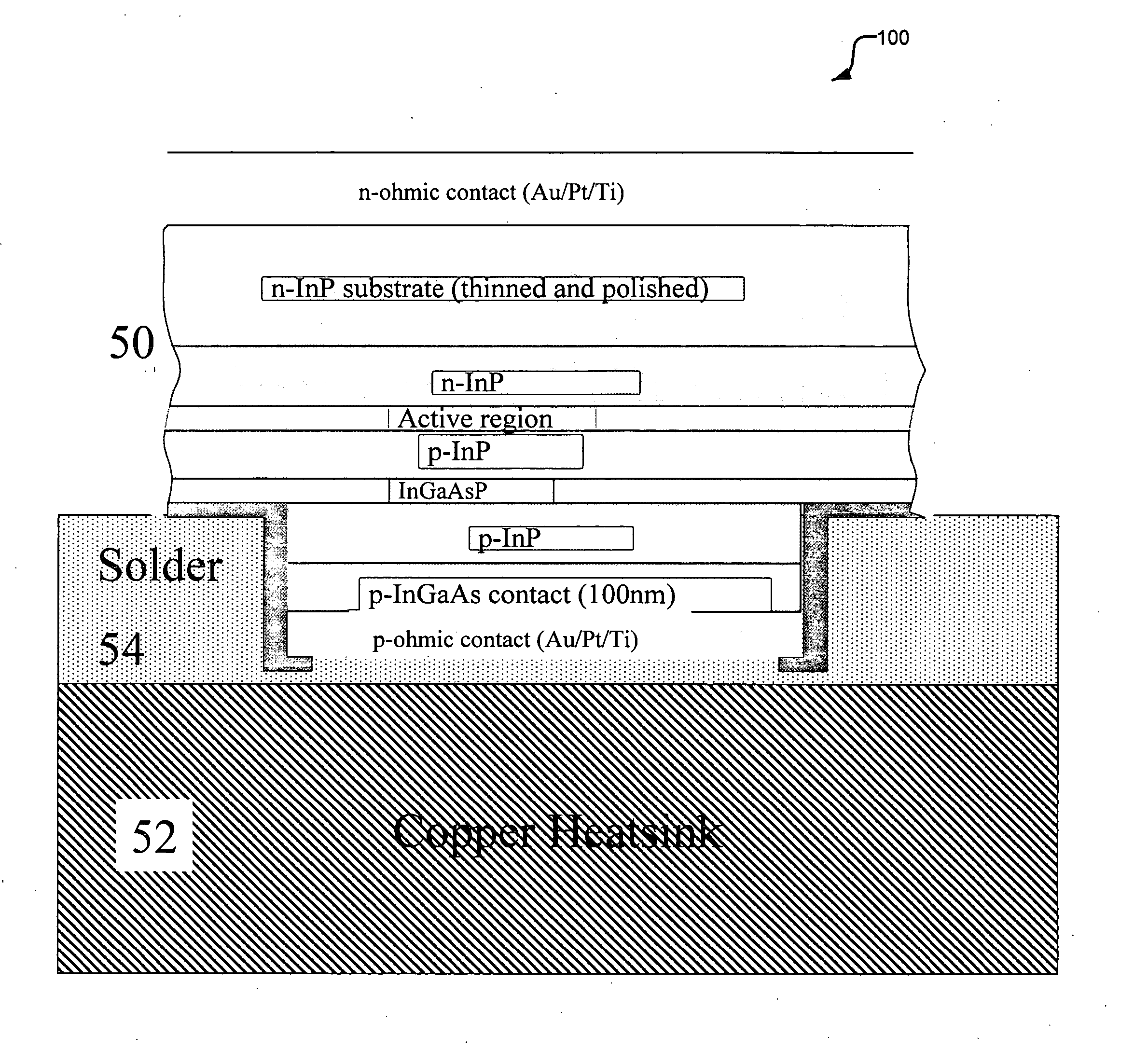
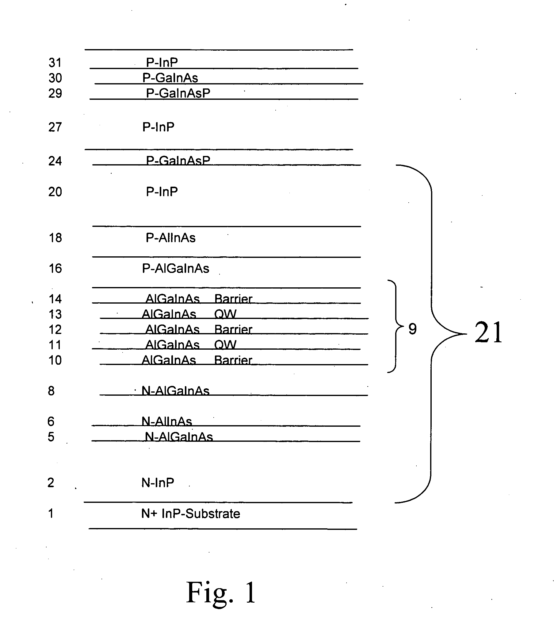
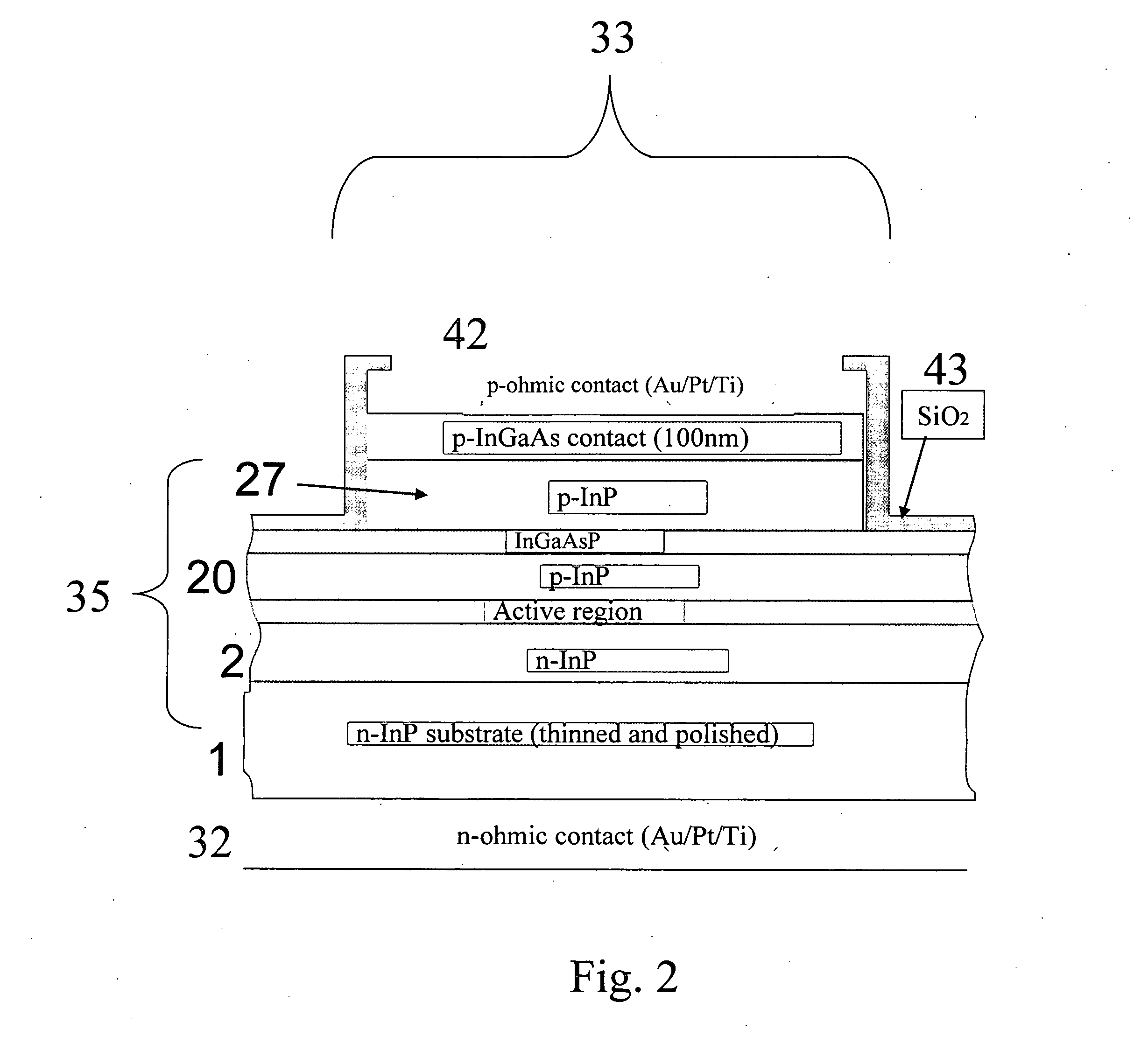
[0023]FIG. 1 shows the layer structure of a semiconductor light emitting device that has been constructed according to the principles of the present invention.
[0024] Specifically, a listing of the epitaxial structure shown. It was fabricated or prepared using conventional III-V compound semiconductor epitaxial growth techniques such as metal organic chemical vapor deposition OMCVD (also referred to as MOCVD) and molecular beam epitaxy (MBE). The starting substrate 1 is n-type InP, on to which the sequence of layers is epitaxially grown using known methods.
[0025] Beginning from the substrate 1, a 1 micrometer thick n+InP lower cladding layer 2 with a silicon (Si) doping concentration of 3×1018 cm−3 is grown followed by a transition region 15 nm thick of lattice matched, graded (Al0.68Ga0.32)0.47In0.53As to Al0.48In0.52As 5-6 into the separate confinement heterostructure (SCH) layers 6-18. Next is the lower graded-index (GRIN) layer 8, which is 45 nm thick beginning with Al0.48In0.5...
PUM
 Abstract
Description
Claims
Application Information