Reflectivity-modulated grating mirror

a reflection-modulated grating mirror technology, applied in the direction of lasers, laser details, electrical equipment, etc., can solve the problems of difficult to increase the speed or reduce the energy consumption, the energy per bit of 357 fj/bit is remarkably small, and the transmission speed of the building block device is high, so as to achieve low power consumption, improve the obtainable data rate, and reduce the effect of energy consumption

Inactive Publication Date: 2014-08-07
DANMARKS TEKNISKE UNIV
View PDF2 Cites 11 Cited by
  • Summary
  • Abstract
  • Description
  • Claims
  • Application Information

AI Technical Summary

Benefits of technology

[0037]In a further aspect, the invention provides optical interconnects comprising one or more VCLs according to the first aspect of the invention for generation of optical data signals based on received electric data signals. The optical interconnects may be implemented in on-chip level as well as the off-chip level. Such optical interconnects may solve most limitations of the current electrical interconnects such as energy consumption problem, crosstalk, speed limitation, channel density limitation, and high-speed clocking limitation. Compared to existing laser sources for chip-level optical interconnects, the laser sources according to the present invention involve the advantages of higher obtainable data rates and much lower energy consumption.
[0038]The basic idea of the invention is to make a grating mirror of which the reflectivity can be modulated, and to apply this reflectivity-modulated grating mirror to modulate the emission of a VCL. By modulating an electrical field of an electrooptic material in the grating mirror, the refractive index and ultimately the reflectivity of the grating mirror can be modulated very fast based on the QCSE. As only the electrical field is to be modulated with virtually no current flow, and as the layer over which it is applied can be made very thin, very low power consumption and high modulation speeds can be achieved.

Problems solved by technology

In short-distance optical interconnects applications, low energy consumption as well as high transmission speed of the building block devices is becoming the key technological issues as the data transmission bandwidth increases.
The demonstrated energy per bit of 357 fJ / bit (=12.5 mW / 35 Gb / s) is remarkably small but is not sufficient for the aforementioned applications.
The weakness of this approach is that it is difficult to further increase the speed or reduce the energy consumption: Speed of a laser diode is decided by its intrinsic response and circuit response.
Regarding the injection current, if one increases the current for a higher intrinsic speed, it will result in higher energy consumption.
On the other hand, if one decreases the current for smaller energy consumption, it will result in slower intrinsic speed.
Thus, it is difficult to further increase the speed and decrease the energy consumption simultaneously in the conventional VCSEL structure.
One should also consider that high injection current is detrimental to long-time stability of small-volume lasers.
Thus, a significant improvement in speed related to parasitic circuit terms is not expected.
Since no modulation occurs in the laser part, current injection to the laser part can be small, resulting in small energy consumption of the laser part.
Thus, if the energy consumption of the modulator part is small as well, the energy consumption of the whole structure including both the laser and modulator parts can be low.
In addition, another limitation that needs to be noted is that this approach of using a DBR which embeds an electrooptic material is not feasible for long wavelength VCSELs (wavelength 1310 nm): In order to obtain a sufficient contrast in reflectivity at a lasing wavelength of interest, the stopband widths of the passive DBR without an electrooptic material and the active DBR with an electrooptical material should be almost same.

Method used


Image

  • Reflectivity-modulated grating mirror
  • Reflectivity-modulated grating mirror
  • Reflectivity-modulated grating mirror

Examples


Embodiment Construction

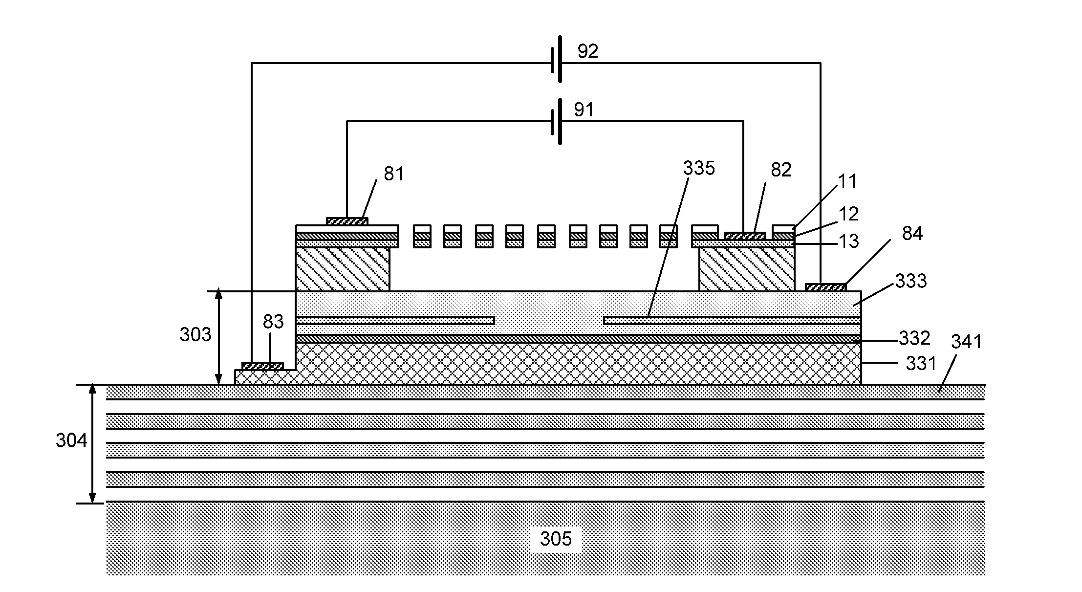
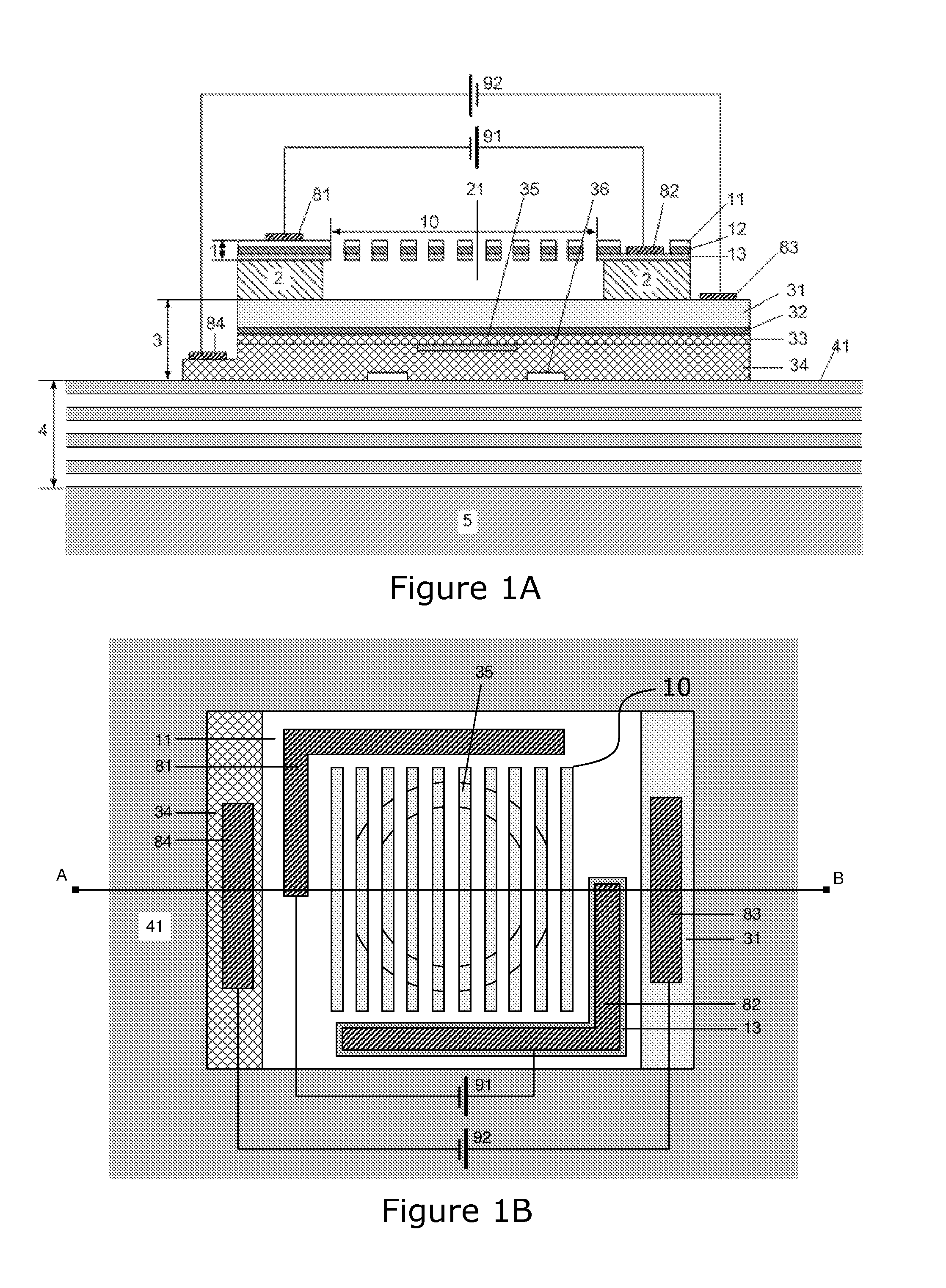
[0056]FIGS. 1A and 1B show cross-sectional side- and top views of an example of the invention, respectively. In this embodiment, the device consists of a grating mirror 1 having an embedded electrooptic material 12 and a grating structure 10, an air gap 21 (or sacrificial layer 2), an active region 3, and a DBR 4 all held by substrate 5. Light is generated in the active material 32 which is typically QWs, is vertically amplified between the grating mirror 1 and the DBR 4, and is emitted through the grating mirror 1. The forward bias 92 for light generation is applied between the p contact 84 and the n contact 83. The injected current flows through the n-doped layer 34, the tunnel junction 35, the p-doped layer 33, the active material 32, and the n-doped layer 31. The reflectivity of the grating mirror 1 is modulated to modulate light emission. The reverse bias 91 is applied between the p contact 81 and the n contact 82. Thus, a strong electric field is induced in the electrooptic ma...


PUM


Abstract

The invention relates to vertical cavity lasers (VCL) incorporating a reflectivity-modulated grating mirror (1) for modulating the laser output. A cavity is formed by a bottom mirror (4), an active region (3), and an outcoupling top grating mirror (1) formed by a periodic refractive index grating region in a layer structure comprising a p- and a n-doped semiconductor layer with an electrooptic material layer (12) arranged there between. The grating region comprises a grating structure formed by periodic perforations to change the refractive index periodically in directions normal to the oscillation axis. A modulated voltage (91) is applied in reverse bias between the n- and p-doped layers to modulate the refractive index of the electrooptic material layer (12) and thereby the reflectivity spectrum of the grating mirror (1). The reflectivity of the grating mirror (1) can be modulated between a reflectivity with little or no out coupling and a reflectivity with normal out coupling, wherein lasing in the VCL is supported at both the first and the second reflectivity. As the out coupling mirror modulates the output, the lasing does not need to be modulated, and the invention provides the advantage of lower power consumption at high modulation speeds.

Description

FIELD OF THE INVENTION[0001]The present invention relates to a vertical cavity laser (VCL) incorporating a grating mirror of which the reflectivity can be modulated to modulate the laser output power.BACKGROUND OF THE INVENTION[0002]In short-distance optical interconnects applications, low energy consumption as well as high transmission speed of the building block devices is becoming the key technological issues as the data transmission bandwidth increases. Thus, the figure of merit is energy consumption per transmitted bit. According to a recent technology roadmap provided in D. A. B. Miller, “Device requirements for optical interconnects to silicon chips”, Proceedings of the IEEE, vol. 97, p. 1166 (2009), a few 10s fJ / bit is required in 2015-2020 for light transmitters of chip-level optical interconnects.[0003]As light emitter, vertical-cavity surface-emitting lasers (VCSELs) are one of the preferable existing solutions. This is because their fabrication technology is matured and ...

Claims


Application Information

Patent Timeline
Patent Type & Authority Applications(United States)
IPC IPC(8): H01S5/183
CPCH01S5/18302H01S5/0655H01S5/18311H01S5/18316H01S5/18325H01S5/18327H01S5/18341H01S5/18366H01S5/18386H01S5/3095H01S5/11H01S5/10H01S5/183
Inventor CHUNG, IL-SUG
Owner DANMARKS TEKNISKE UNIV
Why Eureka
Try Eureka