Phase modulating system
a phase modulating system and phase modulation technology, applied in the field of phase modulation, can solve the problems of difficult to implement the large number of small delays, require a very fast processing, and implement a fully analog phase shifter. achieve the effect of high modulation speed and high resolution
- Summary
- Abstract
- Description
- Claims
- Application Information
AI Technical Summary
Benefits of technology
Problems solved by technology
Method used
Image
Examples
first embodiment
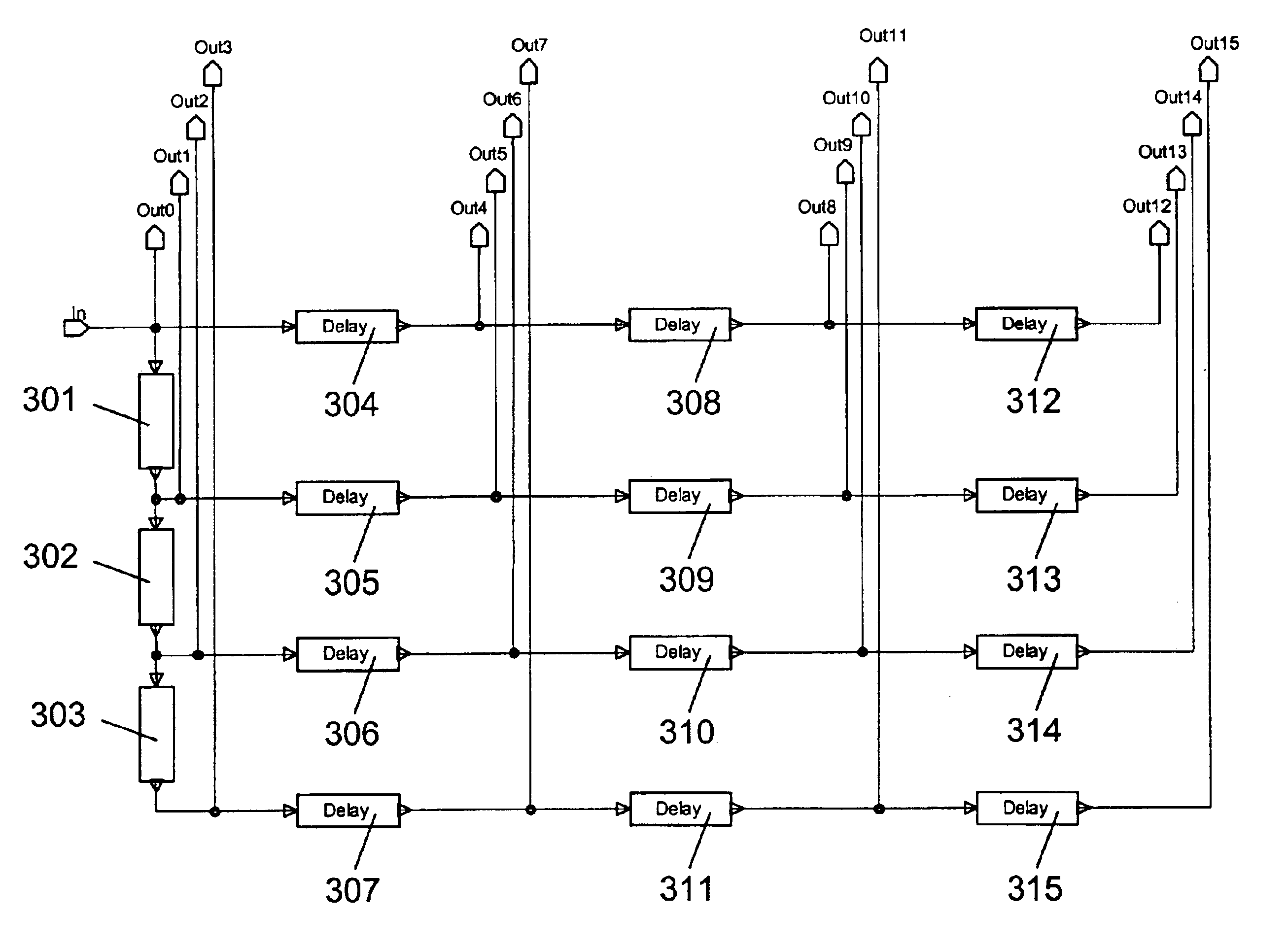
[0051]a phase modulating system according to the invention is presented in the schematic block diagram of FIG. 3. This embodiment is based on the use of a delay matrix as a delay line, in order to reduce the required number of very short delays.
[0052]The phase modulating system of FIG. 3 is a 4-bit system, in which a clock generator (not shown) is connected to an input ‘In’ of a delay matrix. The clock generator generates a clock signal having a period of Tc. Thus, 16 signals which are delayed in steps of Tc / 16 are required.
[0053]Within the delay matrix, the input ‘In’ is connected to a delay element 301, which is further connected to a delay element 302, which is further connected to a delay element 303.
[0054]The input ‘In’ is moreover connected to a delay element 304, which is further connected to a delay element 308, which is further connected to a delay element 312. The output of the delay element 301 is moreover connected to a delay element 305, which is further connected to a ...
second embodiment
[0062]a phase modulating system according to the invention is presented in the schematic block diagram of FIG. 4. This embodiment is based on the use of digital frequency dividers for constructing a delay line, in order to avoid the necessity of very short delays.
[0063]The phase modulating system of FIG. 4 is a 4-bit system. It comprises a clock generator (not shown), the output of which is connected to the input ‘In’ of a phasing arrangement with cascaded frequency dividers. The input signal frequency, provided e.g. by an oscillator, can be tuned as desired. The frequency dividers can be for example D flip-flops DFF, but other suitable circuits could be used as well.
[0064]More specifically, the input ‘In’ of the phasing arrangement is connected to the input of a first digital frequency divider 41 forming a first divide-by-two frequency division stage.
[0065]A first output of the first digital frequency divider 41 is connected to an input of a second digital frequency divider 42 and ...
fourth embodiment
[0083]a phase modulating system according to the invention is presented in the schematic block diagram of FIG. 6. This embodiment is based on approximating part of an n-bit control signal for reducing the number of very short delays. By way of example, n is assumed to be equal to 8.
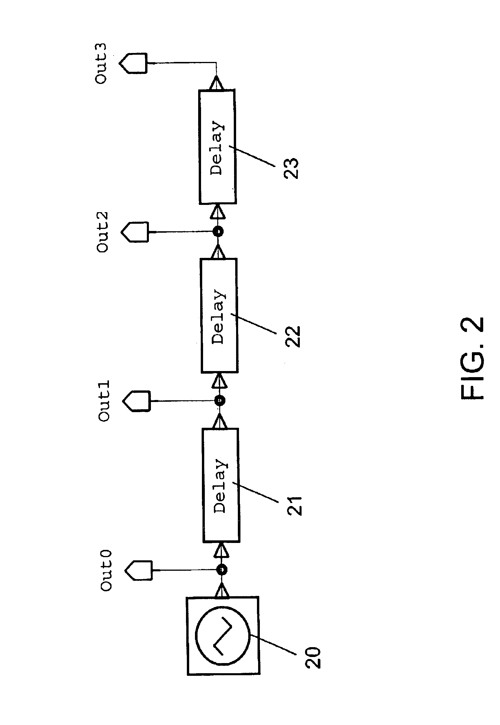
[0084]The phase modulating system of FIG. 6 comprises a clock generator 60, the output of which is connected to a delay line 61. The delay line 61 comprises 2k−1 delay elements connected in series, similarly as depicted in FIG. 2. The parameter k represents the number of most significant bits of the n-bit control signal. By way of example, k is assumed to be equal to 4, thus the delay line 61 comprises 15 delay elements. The input to the first delay element and the output of each of the delay elements are provided to a signal input of a switch 62. Alternatively, the delay line 61 could be realized in any other suitable manner providing a corresponding number of delayed signals, e.g. by the arrangement bet...
PUM
 Abstract
Description
Claims
Application Information


