Circuit component built-in module and method for manufacturing the same

a technology of circuit components and built-in modules, which is applied in the direction of manufacturing tools, printed element electric connection formation, and association of printed circuit non-printed electric components, etc., can solve the problems of short circuit between wires and the inability of conventional circuit component built-in modules to employ low-cost mounting techniques, and achieve the effect of eliminating short circuit and low cos

Inactive Publication Date: 2005-03-03
PANASONIC CORP
View PDF6 Cites 63 Cited by
  • Summary
  • Abstract
  • Description
  • Claims
  • Application Information

AI Technical Summary

Benefits of technology

[0007] Therefore, with the foregoing in mind, it is an object of the present invention to provide a circuit component built-in module that uses a low cost mounting technique such as wire bonding and also can eliminate a wire failure or short circuit, and a method for manufacturing the circuit component built-in module.

Problems solved by technology

Consequently, the wires are separated and moved, resulting in a short circuit between the wires.
As described above, the conventional circuit component built-in module cannot employ a low cost mounting technique such as wire bonding, which has been used widely as a general method for mounting a semiconductor of a circuit component built-in module.

Method used


Image

  • Circuit component built-in module and method for manufacturing the same
  • Circuit component built-in module and method for manufacturing the same
  • Circuit component built-in module and method for manufacturing the same

Examples


example 1

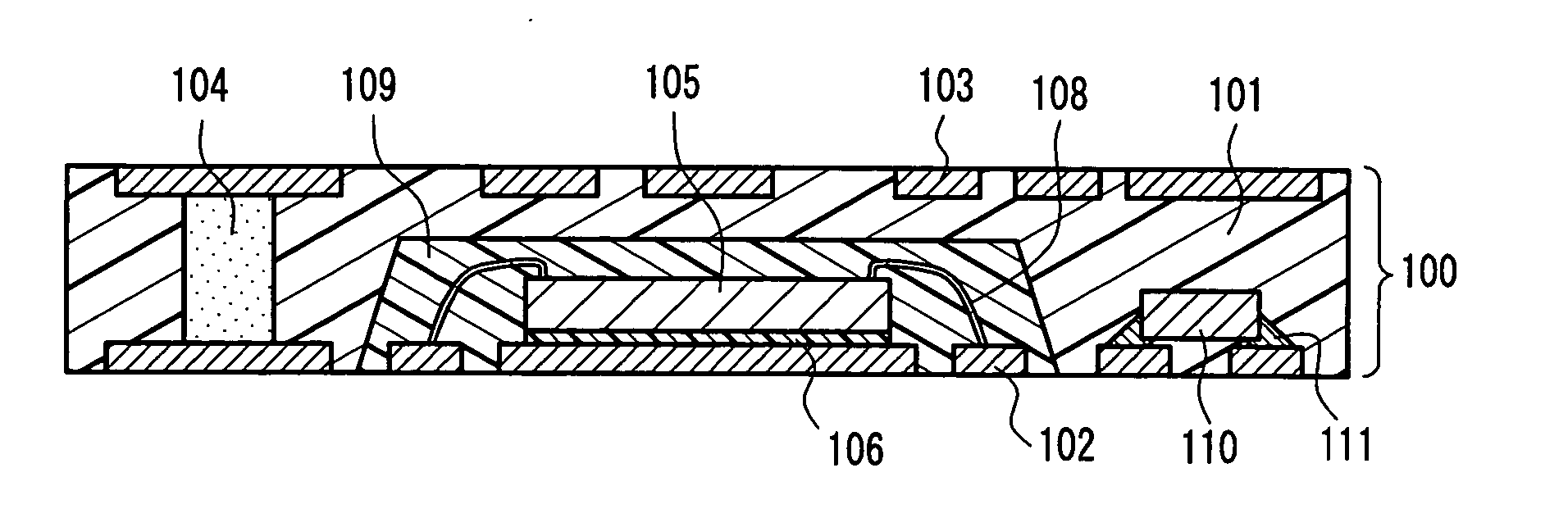
[0065] Example 1 of the present invention will be described by referring to FIGS. 1 to 5. FIGS. 1 to 5 are cross-sectional views showing the configuration of a circuit component built-in module of this example. In FIG. 1, reference numeral 100 is a circuit component built-in module, 101 is a composite material (a first mixture), and 102 and 103 are wiring patterns. The composite material 101 includes a filler and a thermosetting resin. In this case, 15 wt % of liquid epoxy resin (“EF-450” produced by Japan Rec Co., Ltd.) is used as the thermosetting resin, and 85 wt % of alumina powder (“AS-40” produced by SHOWA DENKO K. K., which is spherical with an average particle size of 12 μm) is used as the inorganic filler. Reference numeral 104 is vias for electrically connecting the wiring patterns 102 and 103. Reference numeral 105 is a semiconductor chip (a circuit component) contained in the circuit component built-in module 100. Reference numeral 106 is a die bond (“QMI527” produced by...

example 2

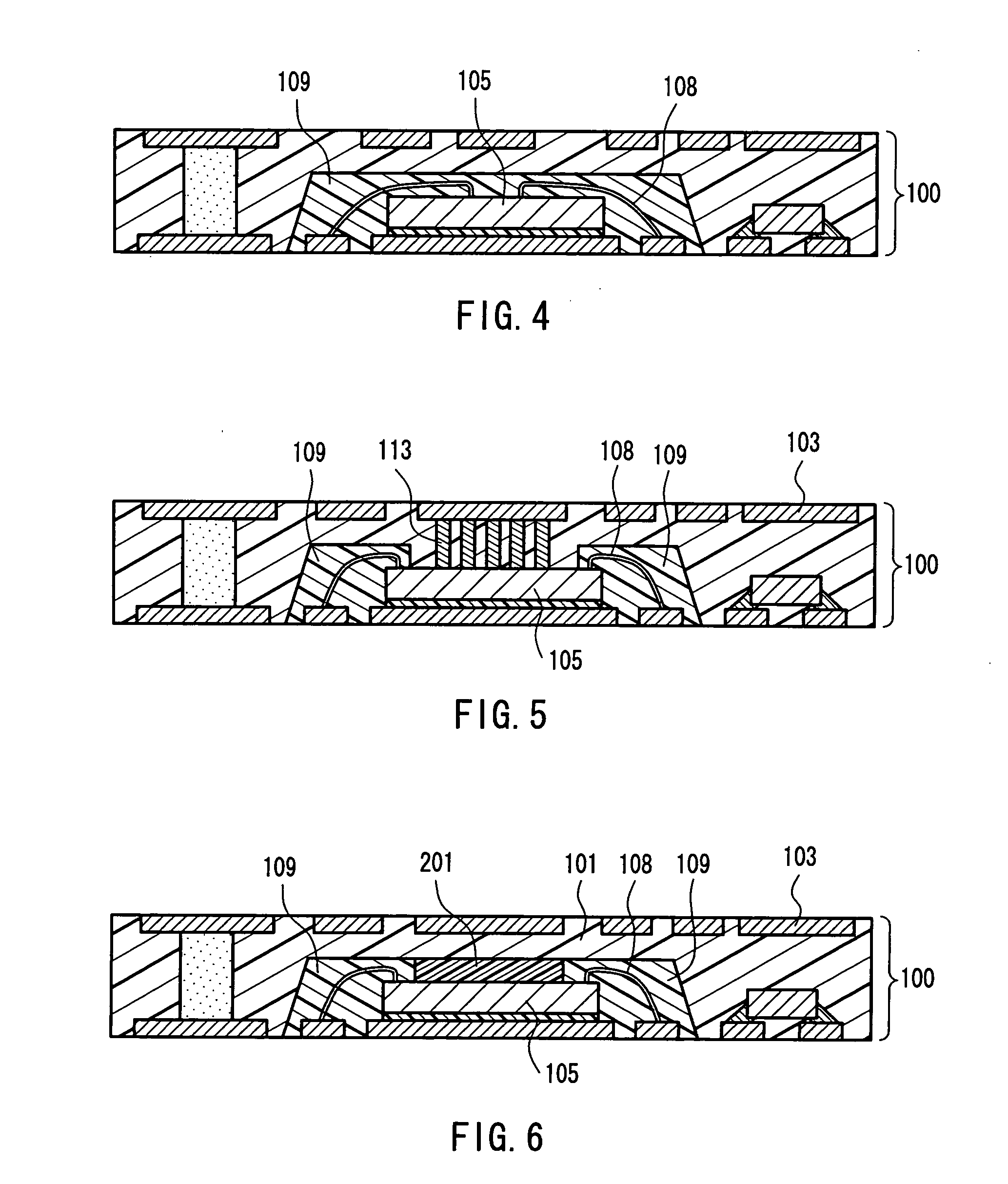
[0076] Example 2 of the present invention will be described by referring to FIGS. 6 to 10. FIGS. 6 to 10 are cross-sectional views showing the configuration of a circuit component built-in module of this example. FIG. 6 differs from FIG. 1 in that a high thermal conductive sealant 201 is arranged between the sealant 109, the semiconductor chip 105, and the composite material 101. The high thermal conductive sealant 201 includes 10 wt % of liquid epoxy resin as a liquid thermosetting resin and 90 wt % of alumina powder as an inorganic filler. In this example, the connection terminals are located on the periphery of the semiconductor chip 105. When the high thermal conductive sealant 201 is arranged in the central portion of the semiconductor chip 105, heat generated from the semiconductor chip 105 can be transferred efficiently.

[0077] The periphery and the central portion of the semiconductor chip 105 need not be considered as precise positions. The same effect can be obtained as lo...

example 3

[0084] Example 3 of the present invention will be described by referring to FIGS. 11 to 15. FIG. 11 is a cross-sectional view showing the shape of a filler included in the composite material 101 of a circuit component built-in module of this example. There is a hollow 302 inside the filler, and a resin outer wall 303 defines the hollow 302. FIG. 12 shows the composite material 101 in which a hollow filler 301 is dispersed. In this case, the outer wall of the hollow filler 301 is made of acrylic resin, the porosity is about 50%, and the average particle size is 20 μm. Other materials, dimensions and porosities may be useful.

[0085] When a component is mounted on the circuit component built-in module as shown in FIG. 1 by reflowing, or when the circuit component built-in module is mounted on a substrate, the semiconductor chip 105 or the chip component 110 may be degraded at 220° C. to 250° C. or more, and the solder 111 in the connecting portion may be remelted to cause a short circu...


PUM


Abstract

A circuit component built-in module includes the following: an electrical insulating substrate made of a first mixture including a filler and a thermosetting resin; a wiring pattern formed on at least a principal surface of the electrical insulating substrate; circuit components that are arranged inside the electrical insulating substrate and connected electrically to the wiring pattern; and vias for electrically connecting the wiring patterns. At least one of the circuit components is mounted using wires. Part or all of the wires is sealed with a second mixture including a filler and a resin. This circuit component built-in module can eliminate a wire failure or short circuit while using a low cost mounting technique such as wire bonding.

Description

BACKGROUND OF THE INVENTION [0001] 1. Field of the Invention [0002] The present invention relates to a circuit component built-in module that contains an active component such as a semiconductor and a passive component such as a capacitor and a method for manufacturing the circuit component built-in module. [0003] 2. Description of the Related Art [0004] With recent advances in small high-performance electronic equipment, there has been a growing demand for a semiconductor having high density and high performance. This also requires a circuit board that can achieve a smaller size and a higher density. Accordingly, a circuit component built-in module has been proposed that includes active and / or passive components and vias for electrically connecting those components and wiring patterns. Moreover, when circuit components are contained in a substrate, it is necessary to improve the heat dissipation or to adjust the thermal expansion coefficients of the substrate and the circuit compon...

Claims


Application Information

Patent Timeline
Patent Type & Authority Applications(United States)
IPC IPC(8): H01L23/31H01L23/433H01L25/16H05K1/18H05K3/20H05K3/40H05K3/46
CPCH01L23/3135H01L23/4334H01L2924/1815H01L2225/06558H01L2924/01019H01L2224/73265H01L2224/32245H01L2224/16245H01L24/48H01L2224/45144H05K2203/049H05K2201/0187H05K3/4614H05K3/4069H05K3/20H05K1/187H01L2924/3025H01L2924/19041H01L2924/01079H01L2924/01078H01L2924/01046H01L25/165H01L2223/6622H01L2224/32145H01L2224/48227H01L2224/48247H01L2224/85001H01L2924/01012H01L2924/00012H01L2924/00H01L2924/00014H01L2224/45015H01L2924/12042H01L2924/181H01L2224/8592H01L2924/19105H01L24/73H01L2224/45124H01L24/45H01L2924/20752H01L2924/20753H01L2924/20754
Inventor ISHIMARU, YUKIHIROSUGAYA, YASUHIROASAHI, TOSHIYUKI
Owner PANASONIC CORP
Why Eureka
Try Eureka