Photodetector and photo detecting system

Inactive Publication Date: 2005-03-03
KK TOSHIBA
View PDF17 Cites 15 Cited by
  • Summary
  • Abstract
  • Description
  • Claims
  • Application Information

AI Technical Summary

Benefits of technology

[0038] Since this photodetector can be produced by an inexpensive and simple producing process, it is possible to provide a high-performance optical detecting system at low costs. Since this photodetector can have a wavelength selectivity, only a predetermined wavelength component can also be detected in an optical system wherein laser beams of a plurality of wavelengths are arranged on the same optical axis.
[0039] Such a transmission photodetector can also receive light from both surfaces, so that it is possible to provide a detecting optical system capable of being applied to the detection of various position shifts.
[0040] If photo detecting units for selecting a wavelength to carry out a detection are

Problems solved by technology

In addition, by providing the beam splitter 2, it is not possible to avoid shifting the optical axis and generating noises on the wave front of beams to have a bad influence.
Therefore, particularly in measuring systems requiring to propagate beams at a long distance, there is a problem in that it is difficult to adapt such a detecting optical system.
In the current technology, detecting systems for the two wavelengths are often separately constructed, so that it is considered that the construction of the detecting optical system is increasingly complicated with the advance of optical technology.
However, in the reverse transparent electrode optical sensors, color is limited to the band gap of silicon.
In addition, since the see-through optical sensors allow the micropore to transmit light beams, it is not possible to enhance both of transmittance and conversion efficiency, and it is not possible to adjust absorption wavelength.
However, in such a detector, there are problems in that the production costs are high and the light transmittance is low.
In addition, since the spectra of wavelengths of light beams absorbe

Method used


Image

  • Photodetector and photo detecting system
  • Photodetector and photo detecting system
  • Photodetector and photo detecting system

Examples


Embodiment Construction

[0084] Referring now to the accompanying drawings, the preferred embodiments of the present invention will be described below in detail.

First Preferred Embodiment: Transmission Photodetector with Electrode Divided into Four Parts

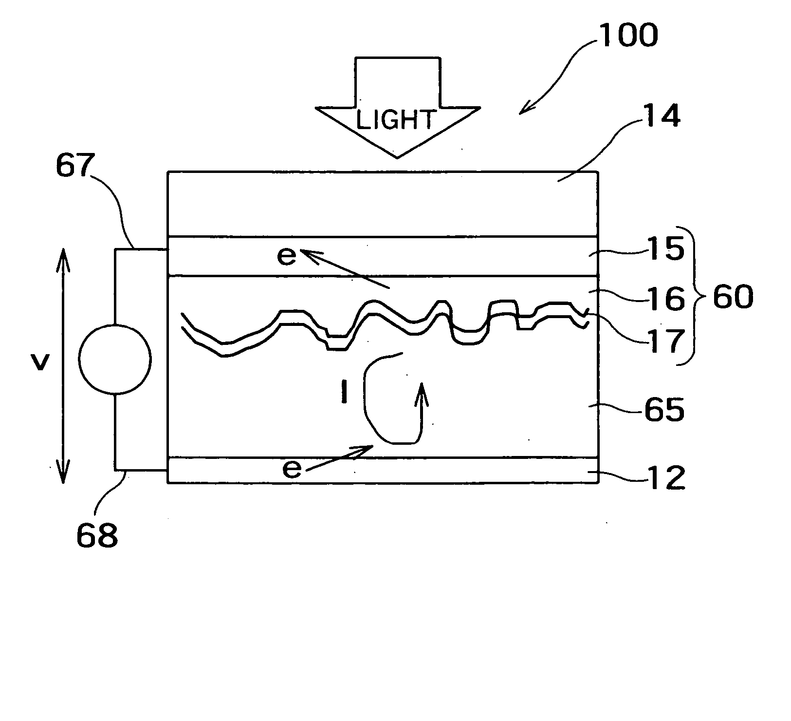
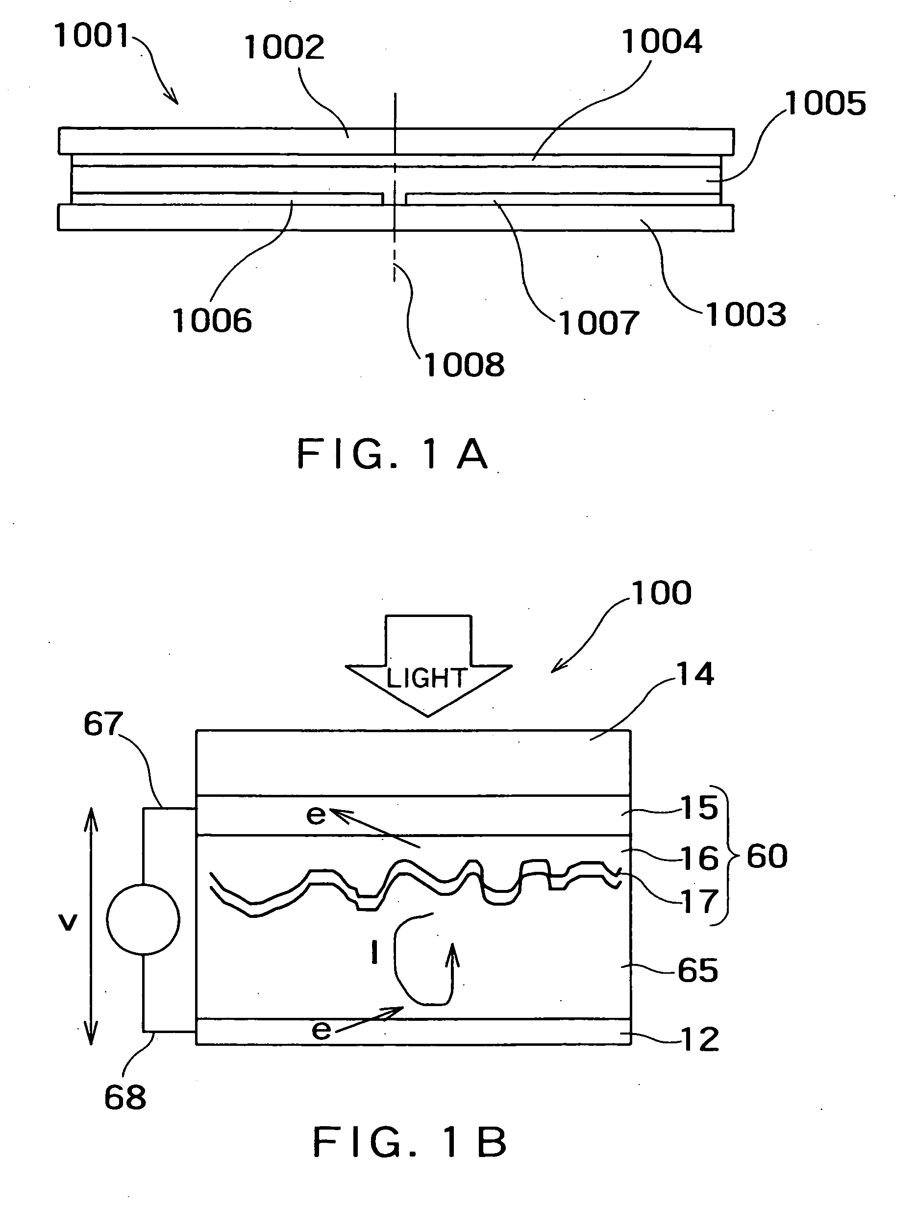
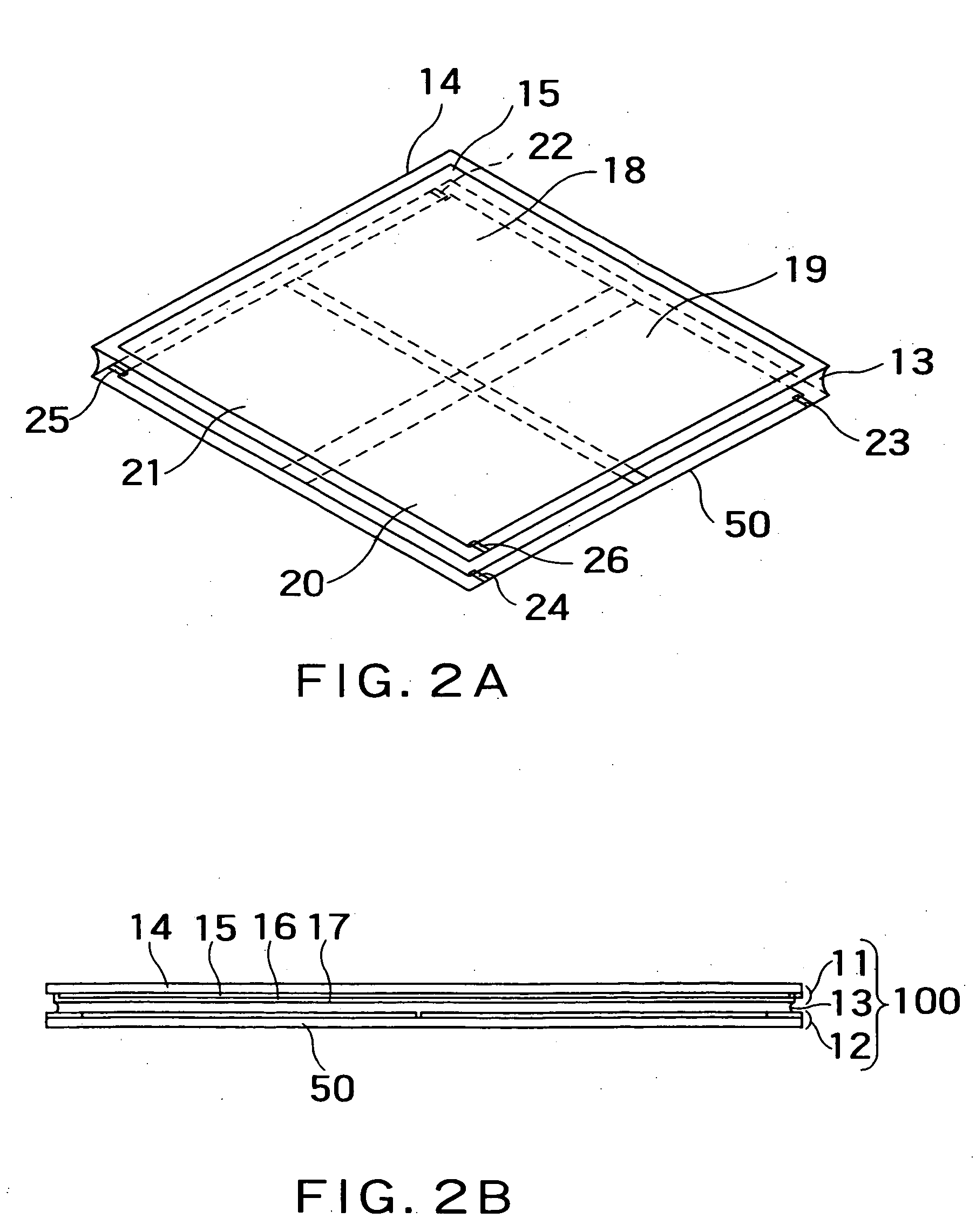
[0085]FIG. 1A is a schematic sectional view showing an example of a basic construction of a preferred embodiment of a photodetector according to the present invention. That is, a photodetector 1001 comprises a first electrode part 1004 formed on a transparent substrate 1002, a second electrode part which is formed on a transparent substrate 1003 and which comprises two divided first and second electrode cells 1006 and 1007, and a photoelectric transfer part 1005 sandwiched between both electrode parts.

[0086] Light beams entering the transparent substrate 1002 pass through the transparent substrate 1002 and the first electrode part 1004 to cause the movement of electrons and positive holes in the photoelectric transfer part 1005. As a result, the electromo...


PUM


Abstract

There is provided a photodetector which has the function of measuring the intensity distribution of light with a simple and inexpensive construction and which has a selectivity for a measured wavelength band. The photodetector comprises a transparent semiconductor electrode part and counter electrode part on each of which a sensitizing dye is applied, and a buffer layer sandwiched therebetween, the counter electrode part or the transparent semiconductor electrode part being divided into a plurality of electrode cells. Thus, it is possible to realize a compact photodetector which carries out a photoelectric transfer using part of light in a wavelength band absorbed into the sensitizing dye and which has a wavelength selectively.

Description

CROSS REFERENCE TO RELATED APPLICATION [0001] This application claims benefit of priority under 35USC §119 to Japanese Patent Application No.2000-95804, filed on Mar. 30, 2000, the contents of which are incorporated by reference herein. BACKGROUND OF THE INVENTION [0002] 1. Field of the Invention [0003] The present invention relates generally to a photodetector and a photo detecting system. More specifically, the invention relates to a photodetector and photo detecting system capable of detecting information about the two-dimensional intensity distribution and wavelength distribution of incident light by the improvement of a transmission photodetector. [0004] 2. Description of Related Art [0005] Now that optical technology is applied to various systems, light receiving elements serving as light detecting means are applied as key devices in applications for all of light applied apparatuses. These light receiving elements are devices which are formed of a semiconductor and which gener...

Claims


Application Information

Patent Timeline
IPC IPC(8): H01L27/30H01L31/00H01L27/14H01L31/10H04N5/335H04N5/351H04N5/369H04N5/372H04N9/07
CPCH01L27/30Y02E10/549H01L51/4226H01L27/307H10K39/00H10K39/32H10K30/151
Inventor YONEZAWA, MINORUSAKURAI, MASATOSHI
Owner KK TOSHIBA
Why Eureka
Try Eureka