Electronics device, semiconductor deivce, and method for manufacturing the same

a semiconductor and semiconductor technology, applied in the field of electronic devices and semiconductor deivce, can solve the problems of shortening between anodes and cathodes, and uneven surface formation of pixel electrodes, so as to prevent the formation of orientation defects of liquid crystals, eliminate unevenness, and high light transmittance

Inactive Publication Date: 2005-03-03
SEMICON ENERGY LAB CO LTD
View PDF20 Cites 74 Cited by
  • Summary
  • Abstract
  • Description
  • Claims
  • Application Information

AI Technical Summary

Benefits of technology

[0025] It is an object of the present invention to provide a high reliable EL display device and a manufacturing method thereof without enlarging the EL display device by shielding intruding moisture or oxygen, which is a factor of deteriorating the property of an EL element.

Problems solved by technology

In a liquid crystal display device, when a pixel electrode is formed over an interlayer insulating film having unevenness, unevenness is also formed on the surface of the pixel electrode along the unevenness of the interlayer insulating film.
The uneven portion has a possibility to cause an orientation defect of a liquid crystal.
However, also in a light emitting device using an EL element, when an anode (or a cathode) is formed over an interlayer insulating film having unevenness, there is a possibility that short is generated between the anode and the cathode since a layer containing an organic compound is thin.
Further, an organic EL element using an organic material for an EL element has a problem that luminescence properties such as luminance or evenness of luminescence significantly deteriorate compared to an early period.
The low reliability is a factor causing the practical application to be limited.
In an EL display device (panel) using an EL element, moisture intruding inside cause a severe reliability lowering to generate a dark spot, shrink or luminance deterioration from the periphery of a light emitting display device.
Briefly, moisture which causes deterioration such as a dark spot intrudes into a display device after sealing in most cases.
It is thought that various deterioration such as internal contamination of an EL display device, deterioration of electric property, a dark spot or shrink.

Method used


Image

  • Electronics device, semiconductor deivce, and method for manufacturing the same
  • Electronics device, semiconductor deivce, and method for manufacturing the same
  • Electronics device, semiconductor deivce, and method for manufacturing the same

Examples


embodiment 1

[0120] [Embodiment 1]

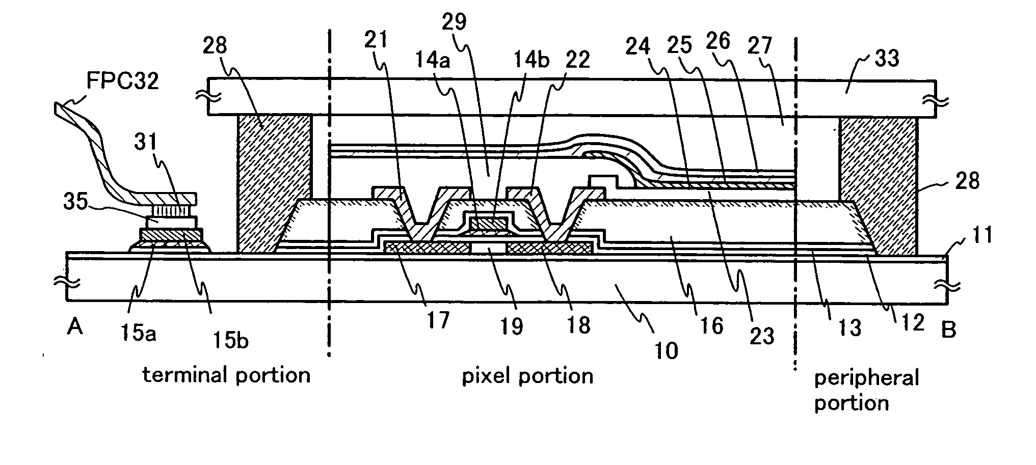
[0121] In this embodiment, an example of an edge portion covered with a metal layer is described with reference to FIGS. 8A and 8B. Portions other than a peripheral portion are identical with those in FIG. 2A shown in Embodiment Mode; therefore, detailed description is omitted here. Note that the same reference numerals are used in FIGS. 8A and 8B for the same parts as those in FIG. 2A.

[0122] Metal layers 621 and 622 are formed by covering a circumference of a high thermostability planarizing film. The metal layers 621 and 622 may be formed simultaneously with source / drain electrodes 21 and 22, or may be separately formed by patterning. However, a part of a lead wiring to be connected to a terminal electrode is not covered with the metal layers 621 and 622, although not shown here.

[0123]FIG. 8B shows an enlarged cross-sectional view of an peripheral portion. A side surface of an edge portion having a step in the high thermostability planarizing film 16 is cove...

embodiment 2

[0126] [Embodiment 2]

[0127] In this embodiment, an example of an edge portion added with an inert element by plasma treatment is described with reference to FIG. 9. Portions other than the edge portion are identical with those in FIG. 2B shown in Embodiment Mode; therefore, detailed description is omitted here. Note that the same reference numerals are used in FIG. 9 for the same parts as those in FIG. 2B.

[0128] This embodiment is an example of forming a highly densified portion on a surface (including a side surface) by adding an inert element without forming an edge portion of a high thermostability planarizing film 16 into a tapered shape.

[0129] In this embodiment, an edge portion of the high thermostability planarizing film 16 is nearly perpendicular, and has curvature in a top edge portion thereof.

[0130] The highly densified portion can be provided on a surface (including a side surface) by a method for adding an inert element with plasma treatment even if an edge portion ha...

embodiment 3

[0133] [Embodiment 3]

[0134] An example of an inversely staggered TFT is described in this embodiment with reference to FIGS. 10A and 10B. Portions other than a TFT and a terminal electrode are identical with those in FIG. 2A shown in Embodiment Mode; therefore, detailed description is omitted here. Note that the same reference numerals as those in FIG. 2A are used in FIGS. 10A and 10B for the same parts as those in FIG. 2A.

[0135] A TFT shown in FIG. 10A is a channel stop type. A gate electrode 719 and a terminal electrode 715 are simultaneously formed, and a semiconductor layer containing an amorphous semiconductor film 714a, an n+ layer 718, and a metal layer 717 are laminated over a gate insulating film 12. A channel stopper 714b is formed over a portion to be a channel formation region of the semiconductor layer 714a. Further, source / drain electrodes 721 and 722 are formed.

[0136] A TFT shown in FIG. 10B is a channel etch type. A gate electrode 819 and a terminal electrode 815 a...


PUM

PropertyMeasurementUnit
grain diameteraaaaaaaaaa
thicknessaaaaaaaaaa
thicknessaaaaaaaaaa

Abstract

It is an object of the present invention to provide a high reliable EL display device and a manufacturing method thereof by shielding intruding moisture or oxygen which is a factor of deteriorating the property of an EL element without enlarging the EL display device. In the invention, application is used as a method for forming a high thermostability planarizing film 16, typically, an interlayer insulating film (a film which serves as a base film of a light emitting element later) of a TFT in which a skeletal structure is configured by the combination of silicon (Si) and oxygen (O). After the formation, an edge portion or an opening portion is formed to have a tapered shape. Afterwards, distortion is given by adding an inert element with a comparatively large atomic radius to modify or highly densify a surface (including a side surface) for preventing the intrusion of moisture or oxygen.

Description

BACKGROUND OF THE INVENTION [0001] 1. Field of Invention [0002] The present invention relates to a semiconductor device having a circuit including a thin film transistor (hereinafter referred to as a TFT), and to a method for manufacturing the same. For example, the invention relates to an electronics device on which an electro-optical device typified by a liquid crystal display panel or a light emitting display device having an organic light emitting element is mounted as its component. [0003] In this specification, the term semiconductor device refers to a device in general that utilizes semiconductor characteristics to function, and electro-optical devices, semiconductor circuits and electronics devices are all included in the semiconductor device. [0004] 2. Description of the Related Art [0005] In recent years, a technique for forming a thin film transistor (a TFT) by using a semiconductor thin film (thickness is about from several nm to several hundreds nm) formed over a substr...

Claims


Application Information

Patent Timeline
Patent Type & Authority Applications(United States)
IPC IPC(8): G02F1/1362G02F1/1368G09F9/00G09F9/30H01L21/77H01L21/84H01L27/12H01L27/32H01L51/50H01L51/52H05B33/04H05B33/10H05B33/22
CPCG02F1/13454G02F1/136227H01L27/12H01L27/1214H01L2251/5323H01L27/3246H01L27/3258H01L51/5246H01L51/529H01L27/3244H01L27/1248H10K59/124H10K59/122H10K59/12H10K50/8426H10K50/87H10K2102/3031
Inventor YAMAZAKI, SHUNPEINAGAI, MASAHARUNAKAMURA, OSAMU
Owner SEMICON ENERGY LAB CO LTD
Why Eureka
Try Eureka