Semiconductor power device with charge compensation structure and monolithic integrated circuit, and method for fabricating it

a technology of monolithic integrated circuits and power devices, applied in the direction of semiconductor devices, electrical devices, transistors, etc., to achieve the effect of improving the isolation of potentials

Active Publication Date: 2005-03-03
INFINEON TECH AG
View PDF4 Cites 67 Cited by
  • Summary
  • Abstract
  • Description
  • Claims
  • Application Information

AI Technical Summary

Benefits of technology

[0037] On account of the corridor with greater distances between the p-type pillars that is provided in the third aspect of the invention, the p-type zones, in the head region of the pillars do not diffuse to such an extent that a shunt that can occur in the second aspect is prevented. Consequently, the third aspect of the invention enables a monolithic integrated circuit to be accommodated in the active zone of the COOLMOS® without restricting the blocking properties of the COOLMOS®. What is more, this structure also does not require additional process steps or mask changes in the lower region with the pillar structure.
[0038] In a further embodiment of the invention, it is provided that a corridor surrounding the monolithic integrated circuit is arranged between the region of the semiconductor power elements and the region of the semiconductor circuit elements, in which corridor the pillars have a smaller diameter than in the region of the semiconductor power elements. In this case, although different masks or masks which are to be newly designed are to be provided for the substructure of the semiconductor power chip, this achieves an improved isolation of the potentials between the surface region of the semiconductor chip with semiconductor circuit elements and the surface region of the semiconductor chip with semiconductor power elements.
[0039] Furthermore, it is provided that the semiconductor circuit elements are surrounded by a complementarily doped frame in the region of the semiconductor circuit elements of the integrated circuit. This has the advantage that the semiconductor circuit elements of the integrated circuit are insulated from the remaining active structure of the COOLMOS® by a pn junction. In this case, the charge compensation structure with its p-conducting pillars does not project into a well made of n-conducting material into the n-conducting well region. The charge compensation cells arranged underneath have p-conducting pillars whose head region is widened below the well in such a way that the cell volume in the head region is also p-conducting and the head regions form a closed p-conducting layer that downwardly delimits the n-conducting well.

Problems solved by technology

On account of the pillar structure of the charge compensation cells that extend over the entire top side and the volume of the semiconductor chip of the semiconductor power device the problem arises of arranging signal-processing and / or controlling, integrated circuits monolithically on the semiconductor chip of the semiconductor power device.
A further problem consists in isolating the region of the semiconductor circuit elements for the integrated circuit from the region of the semiconductor power elements, especially as the drift zone is relatively highly doped in the semiconductor chip with COOLMOS® semiconductor power devices.

Method used


Image

  • Semiconductor power device with charge compensation structure and monolithic integrated circuit, and method for fabricating it
  • Semiconductor power device with charge compensation structure and monolithic integrated circuit, and method for fabricating it
  • Semiconductor power device with charge compensation structure and monolithic integrated circuit, and method for fabricating it

Examples


first embodiment

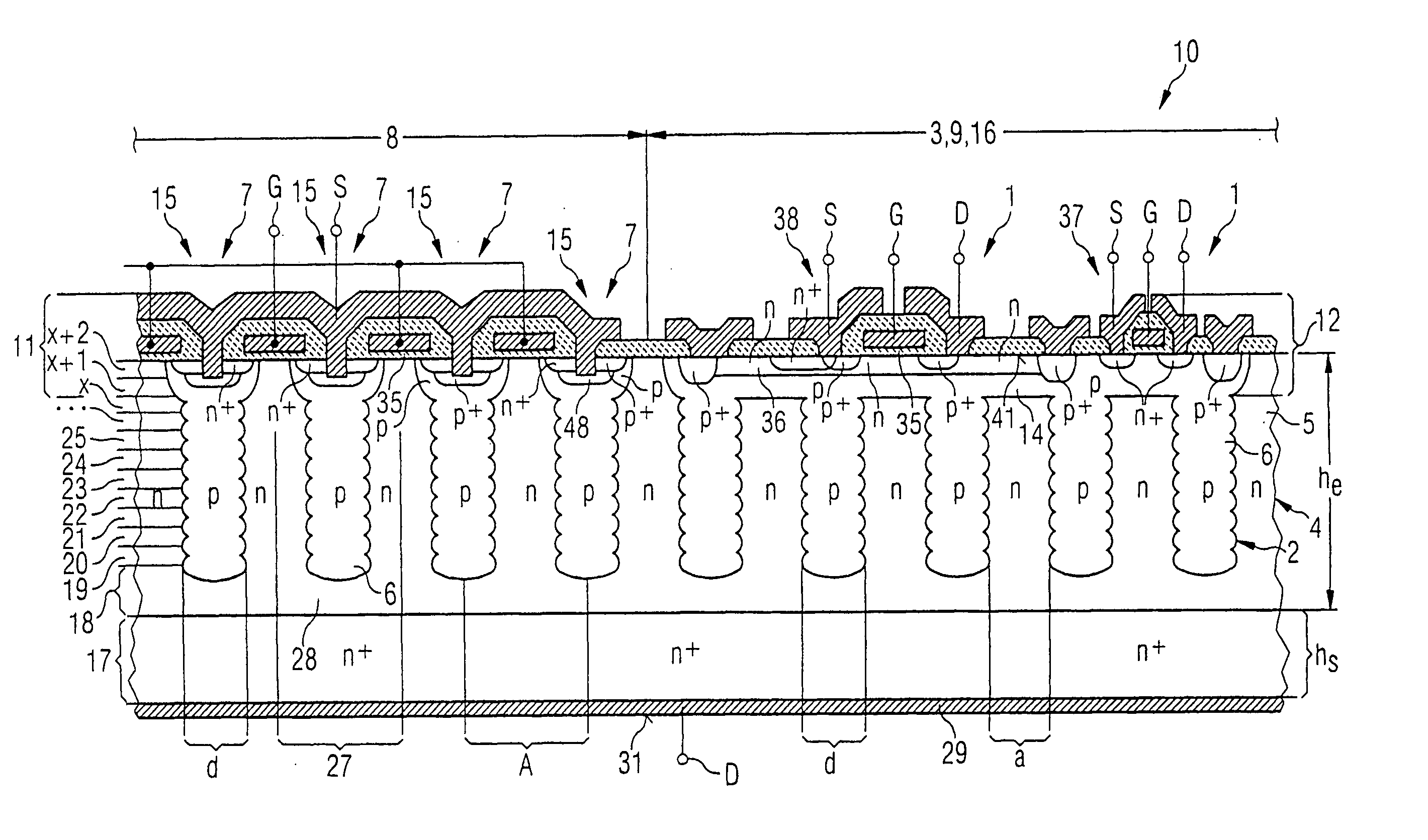
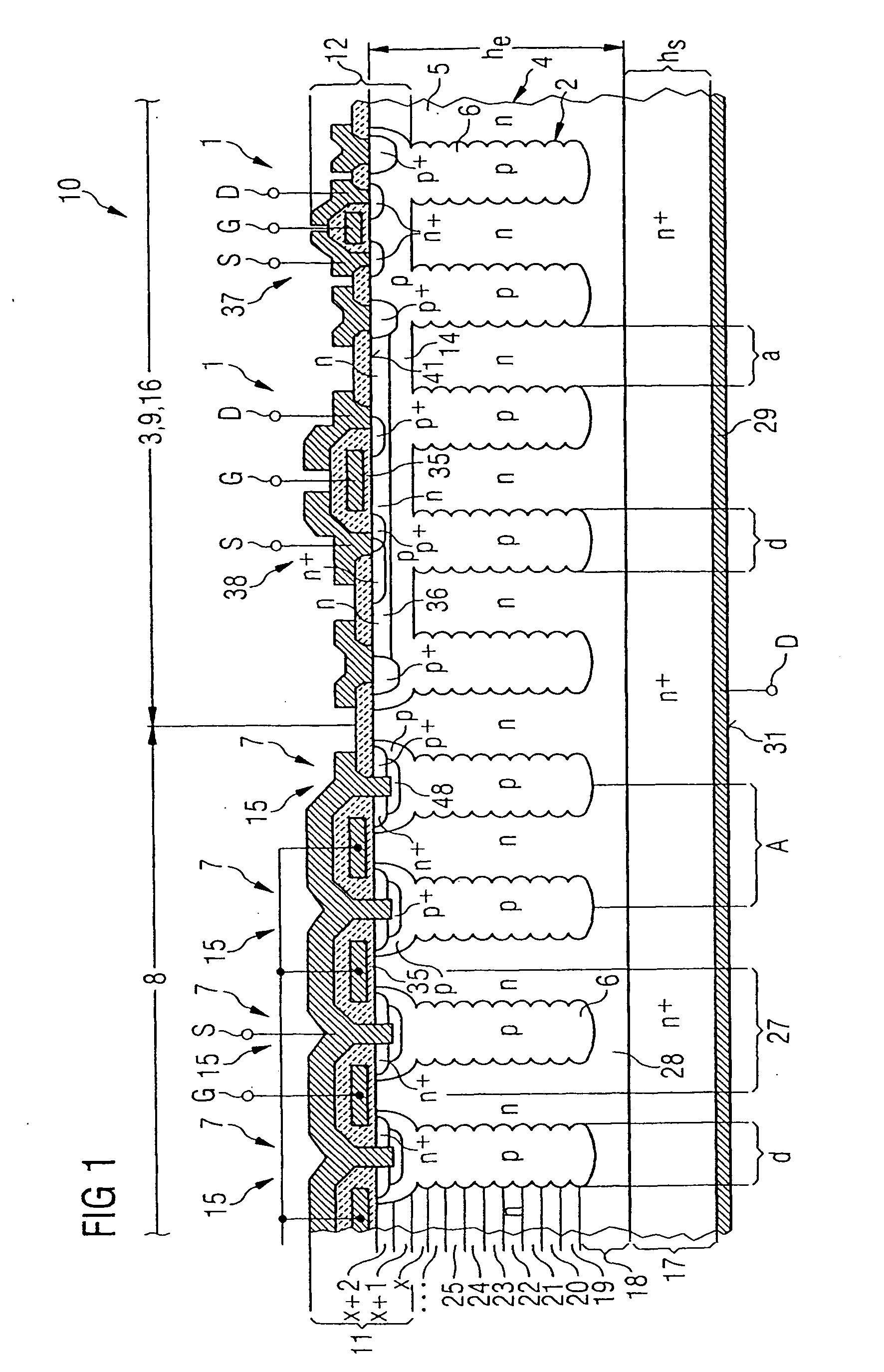
[0072]FIG. 1 shows a diagrammatic cross section through a semiconductor chip 4 of a semiconductor power device 10 of the invention. The semiconductor power device 10 has a charge compensation structure 2. In the semiconductor chip volume 5 above said power compensation structure 2 there are arranged both a region 8 with semiconductor power elements 7 that form a vertical MOS transistor 15 and a region 9 having semiconductor circuit elements 1 of a monolithic integrated circuit 3. In this case, complementarily doped pillars 6 made of p−-conducting monocrystalline material extend in the vertical direction right into surface regions 11 of the semiconductor power components 7.

[0073] The charge compensation structure 2 with its charge compensation cells 27 and the p−-conducting pillars 6 does not project into a surface region 12 for the semiconductor circuit elements 1, but rather touches, with the topmost pillar region, a p−-conducting well 14 that extends over the entire region 9 of th...

second embodiment

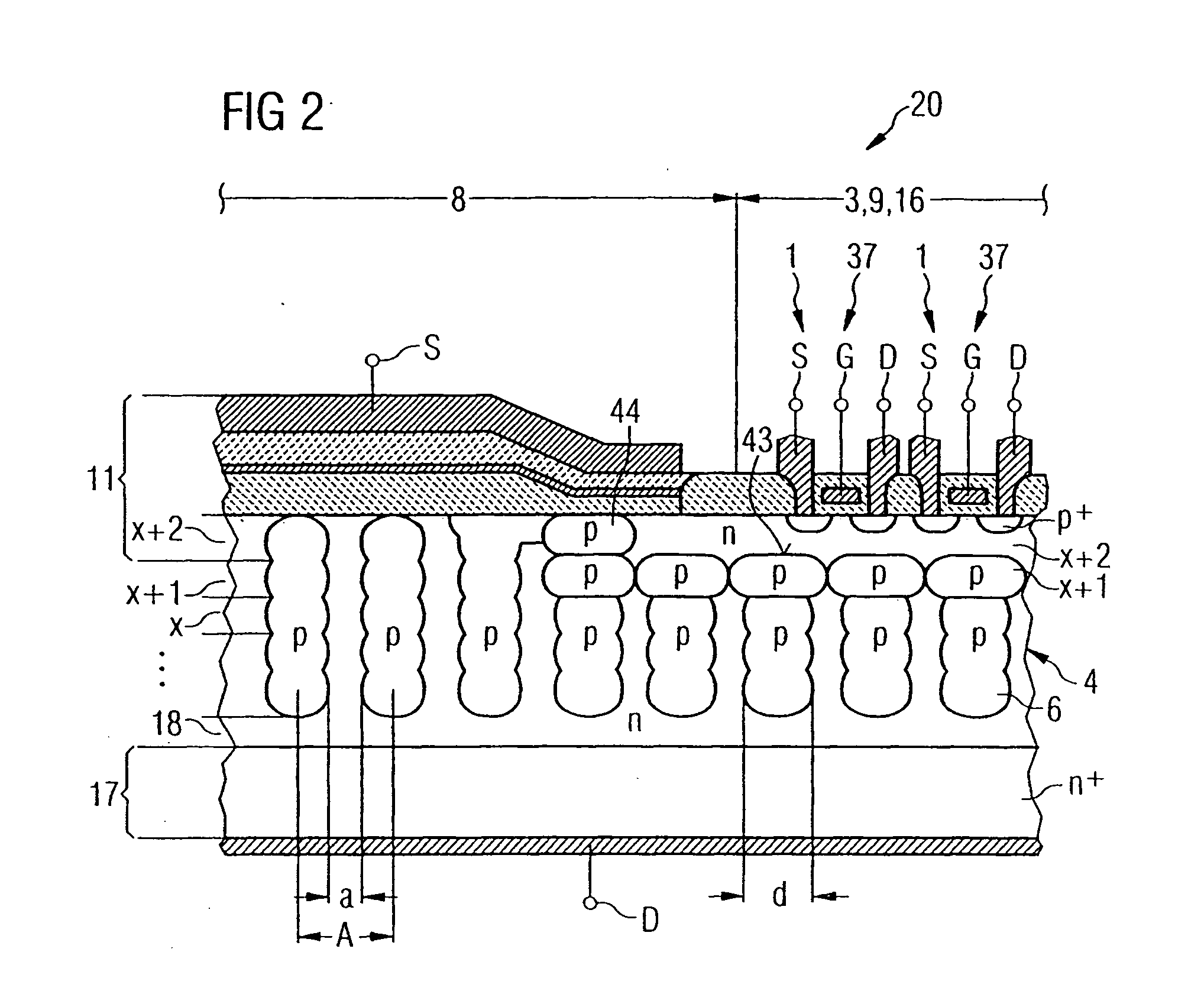
[0079]FIG. 2 shows a diagrammatic cross section through a semiconductor chip 4 of a semiconductor power device 20 of the invention. This cross-sectional view only shows a detail exhibiting the formation of an n-conducting well 36 for a monolithic integrated circuit with p-channel MOS field-effect transistors 38. A schematic sketch of this type for two MOS transistors 37 of this type with source S, gate G and drain D electrodes can be seen at the top right edge of the illustration. The n-conducting well 36 is delimited by a semiconductor structure comprising p-conducting pillars 6, the x+1 epitaxial layer having widened p-conducting zones that are patterned in such a way that the upper regions 42 of the p-conducting pillars 6 of the charge compensation structure 2 touch one another and thus form a closed underside 43 for the n-conducting well 36, while laterally the topmost layer 44 of the p-conducting pillars 6 is likewise widened in such a way as to form a closed edge all around th...

fourth embodiment

[0082]FIG. 4 shows a diagrammatic cross section through a semiconductor chip 4 of a semiconductor power device 40 of the invention. Components with functions identical to those of the previous figures are identified by the same reference symbols and are not discussed in any greater detail. In this case, headless p-conducting pillars 33 are provided in the corridor region 13, the diameter d′ of said pillars being greater than the diameter d of pillar structures that reach as far as the top side of the semiconductor chip in the corridor region B. A charge compensation cell 27 is arranged in the left-hand edge region of the cross section of FIG. 4, the p-conducting pillar 6 of said charge compensation cell having the same diameter d′ as the headless p-conducting pillars 33 in the corridor region 13.

[0083]FIG. 5 shows a diagrammatic plan view of an active top side of a semiconductor chip 4 in accordance with FIG. 4 with a detail from a corridor 13. A plurality of p-conducting pillars 6 ...


PUM


Abstract

The invention relates to a semiconductor power device with charge compensation structure and monolithic integrated circuit, and method for fabricating it. In the case of this semiconductor power device, zones (6) in charge compensation cells (27) that are arranged vertically and doped complementarily to the semiconductor chip volume (5) are arranged in the entire chip volume, the complementarily doped zones (6) extending right into surface regions (11) of the semiconductor power elements (7) and not projecting into surface regions (12) of semiconductor surface elements (1).

Description

PRIORITY [0001] This application claims priority to German application no. 103 40 131.8 filed Aug. 28, 2003. TECHNICAL FIELD OF THE INVENTION [0002] The invention relates to a semiconductor device with charge compensation structure and monolithic integrated circuit on a semiconductor chip, the charge compensation structure having charge compensation cells having pillars in the cells that are arranged vertically and doped complementarily to the semiconductor chip volume or to the cell volume. Furthermore, the invention relates to a method for fabricating the semiconductor power element. BACKGROUND OF THE INVENTION [0003] A semiconductor component with charge compensation structure is disclosed in the document DE 101 32 136 C1. Such charge compensation structures form the basis of COOLMOS® (registered trademark DE 38844786.5) semiconductor power devices. In the case of such semiconductor power devices with the charge compensation structure, p-type and n-type zones below the actual MOS...

Claims


Application Information

Patent Timeline
Patent Type & Authority Applications(United States)
IPC IPC(8): H01L21/336H01L27/088H01L29/06H01L29/76H01L29/78
CPCH01L27/0883H01L29/0634H01L29/7802H01L29/66712H01L29/0646
Inventor AHLERS, DIRKMARION, MIGUEL CUADRONWAHL, UWEWILLMEROTH, ARMIN
Owner INFINEON TECH AG
Why Eureka
Try Eureka