Dicing/die-bonding film, method of fixing chipped work and semiconductor device

a chipped work and bonding film technology, applied in the direction of film/foil adhesives, chemistry apparatus and processes, transportation and packaging, etc., can solve the problems of difficult balance between the abilities, the uniform adhesive layer is hardly formed, and the application of the adhesive requires a special unit and a long time. , to achieve the effect of excellent balan

Inactive Publication Date: 2005-03-03
NITTO DENKO CORP
View PDF16 Cites 54 Cited by
  • Summary
  • Abstract
  • Description
  • Claims
  • Application Information

AI Technical Summary

Benefits of technology

[0009] An object of the present invention is to provide a dicing/die-bonding film comprising a pressure-sensitive adhesive layer on a supporting base material and a die-bonding adhesive layer arranged in a releas...

Problems solved by technology

In this method, however, a uniform adhesive layer is hardly formed, and application of the adhesive requires a special unit and a long time.
However, it is not easy to balance both the abilities.
When sufficient retention is required of the adhesive layer particularly in a system of dicing a semiconductor wafer with a rotating circular tooth, the dicing/die-bonding film satisfying the abov...

Method used


Image

  • Dicing/die-bonding film, method of fixing chipped work and semiconductor device
  • Dicing/die-bonding film, method of fixing chipped work and semiconductor device
  • Dicing/die-bonding film, method of fixing chipped work and semiconductor device

Examples


examples

[0098] Hereinafter, this invention is described in more detail by reference to the Examples. In the following description, “parts” refers to parts by weight. For irradiation with ultraviolet rays, an ultraviolet (UV) irradiation unit (NEL UM-110 (Nitto Seiki Co., Ltd.) was used.

production example

Preparation of a Die-Bonding Adhesive Layer

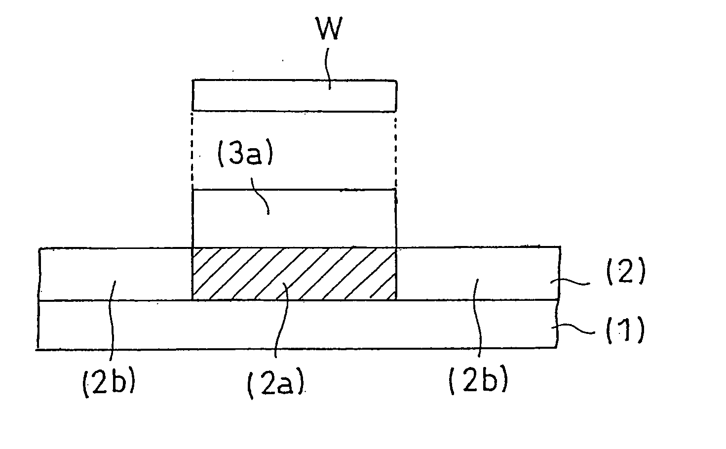
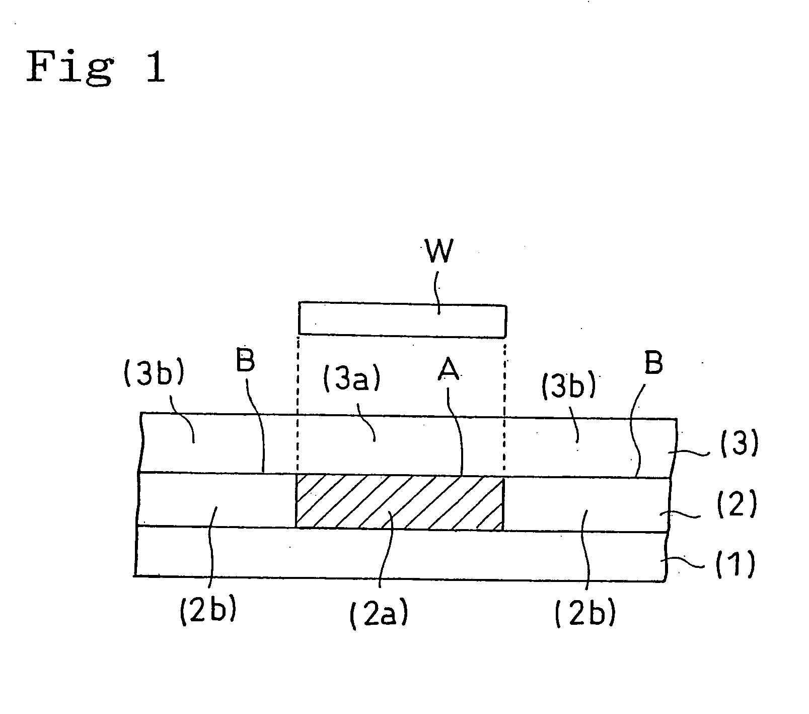
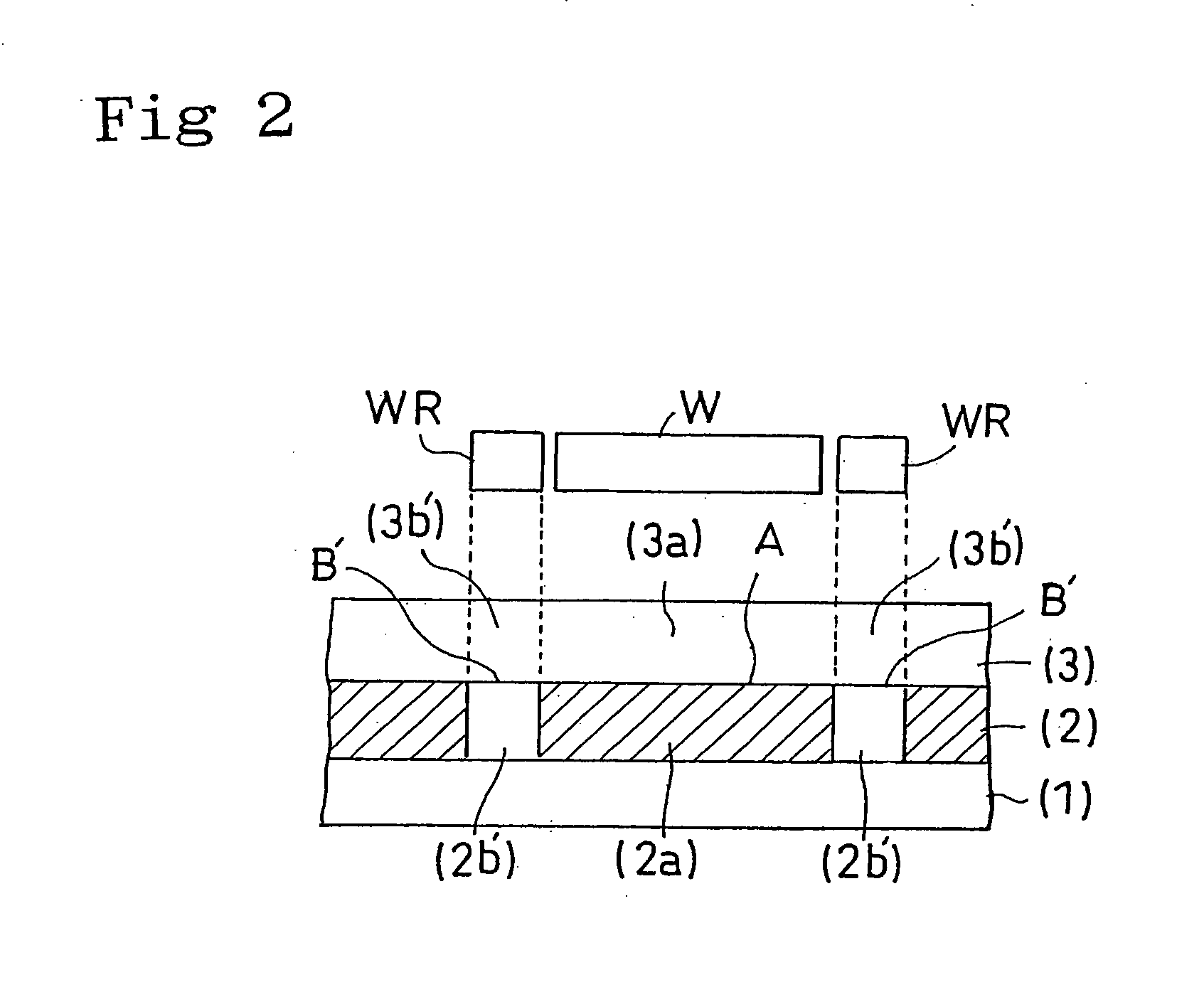
[0099] The components shown in Table 1 below, that is, epoxy resin, phenol resin, acrylic rubber, silica and a curing accelerator were compounded in the ratios shown in the table to prepare compositions for die-bonding adhesives (A) to (C), and each composition was mixed with and dissolved in toluene. The mixed solution was applied onto a polyester film (separator) treated with a releasing agent. Then, the polyester film coated with the mixed solution was dried at 120° C. to remove the toluene, whereby each of the die-bonding adhesive layers A to C of 20 μm in thickness in the B-stage on the polyester film were obtained.

TABLE 1Die-bonding adhesive(parts by weight)CompositionsABCEpoxy resin (a1)24.924.915.5Epoxy resin (a2)24.924.915.5Phenol resin29.229.218Acrylic rubber202050Silica0100100Curing accelerator111

[0100] In Table 1, [0101] is bisphenol A type epoxy resin (epoxy equivalent, 186 g / eq.; viscosity, 10 Pa.s / 25° C.), [0102] is triphe...

example 1

Preparation of a Radiation-Curing Acrylic Pressure-Sensitive Adhesive

[0107] 70 parts of butyl acrylate, 30 parts of ethyl acrylate and 5 parts of acrylic acid were copolymerized in ethyl acetate in a usual manner to give a solution containing an acrylic polymer at a concentration of 30% by weight having a weight-average molecular weight of 800,000. 20 parts of dipentaerythritol monohydroxy pentaacrylate as a photopolymerizable compound and 1 part of α-hydroxy cyclohexyl phenyl ketone as a photopolymerization initiator were compounded with the acrylic polymer solution. The mixture was dissolved uniformly in toluene to prepare a solution containing a radiation-curing acrylic pressure-sensitive adhesive at a concentration of 25% by weight.

[0108] (Preparation of a dicing / Die-Bonding Film

[0109] The above radiation-curing acrylic pressure-sensitive adhesive solution was applied onto a polyethylene film of 60 μm in thickness as the supporting base material and dried to form a pressure-s...


PUM

PropertyMeasurementUnit
Fractionaaaaaaaaaa
Fractionaaaaaaaaaa
Fractionaaaaaaaaaa

Abstract

A dicing/die-bonding film including a pressure-sensitive adhesive layer (2) on a supporting base material (1) and a die-bonding adhesive layer (3) on the pressure-sensitive adhesive layer (2), wherein a releasability in an interface between the pressure-sensitive adhesive layer (2) and the die-bonding adhesive layer (3) is different between an interface (A) corresponding to a work-attaching region (3a) in the die-bonding adhesive layer (3) and an interface (B) corresponding to a part or a whole of the other region (3b), and the releasability of the interface (A) is higher than the releasability of the interface (B). The dicing/die-bonding film is excellent in balance between retention in dicing a work and releasability in releasing its diced chipped work together with the die-bonding adhesive layer.

Description

BACKGROUND OF THE INVENTION [0001] 1. Field of the Invention [0002] The present invention relates to a dicing / die-bonding film. The dicing / die-bonding film is used for subjecting a work to dicing in such a state that an adhesive for sticking a chipped work (semiconductor chip etc.) to an electrode material is arranged on a work (semiconductor wafer etc.) before dicing. Further, this invention relates to a method of fixing a chipped work by using the dicing / die-bonding film. Also, this invention relates to a semiconductor device having a chipped work adhesive-bonded by the fixing method. [0003] 2. Description of the Related Art [0004] A semiconductor wafer on which a circuit pattern was formed is subjected to dice into chipped works (dicing step), as necessary after back-grinding to regulate the thickness. In the dicing step, the semiconductor wafer is generally washed at suitable fluid pressure (usually, about 2 kg / cm2) to remove a cut layer. Then, the chipped work is adhesive-bonde...

Claims


Application Information

Patent Timeline
IPC IPC(8): H01L21/78C09J5/00H01L21/301H01L21/58H01L21/68
CPCC09J7/02Y10T428/218C09J2201/606C09J2201/61C09J2203/326C09J2205/31C09J2433/00H01L21/6836H01L24/27H01L24/83H01L2221/68327H01L2224/274H01L2224/8385H01L2924/01002H01L2924/01004H01L2924/01005H01L2924/01013H01L2924/01015H01L2924/01016H01L2924/01027H01L2924/01029H01L2924/01033H01L2924/01047H01L2924/01074H01L2924/01079H01L2924/01082H01L2924/07802H01L2924/3025H01L24/29H01L2224/2919H01L2224/83191H01L2924/01006H01L2924/01019H01L2924/0665C09J2201/36Y10T428/28Y10T428/2848H01L2924/10253H01L2924/00H01L2924/3512C09J7/20C09J2301/208C09J2301/302C09J2301/304C09J2301/416H01L21/78
Inventor MATSUMURA, TAKESHIMIZUTANI, MASAKI
Owner NITTO DENKO CORP
Why Eureka
Try Eureka