Low-impedance electrical resistor and process for the manufacture of such resistor

a technology of low-impedance electrical resistors and manufacturing processes, which is applied in the manufacture of resistors, resistor details, electrical apparatus, etc., can solve the problems of large variations in resistance values and poor reproducibility, and achieve the effect of maximizing the number of resistors, high resistance values, and high precision and reproducibility of resistors

Inactive Publication Date: 2005-03-03
ISABELLENHUTTE HEUSLER
View PDF18 Cites 8 Cited by
  • Summary
  • Abstract
  • Description
  • Claims
  • Application Information

AI Technical Summary

Benefits of technology

[0011] By means of sawing, a substantially higher precision and reproducibility of the resistors is achieved than with other separation processes such as etching, stamping and, for example, in the case of the use of lasers which itself is another possibility. In addition, it is possible to maximize the number of resistors, which can be manufactured for a given useful surface area by sawing.
[0012] The process is appropriate, among other purposes, for the manufacture of extremely low-impedance resistances, for example, in the range of approximately 0.5 mΩ to 5 mΩ in large scale manufacture, however, it is also possible to manufacture resistors with even lower or with higher resistance values, for example 0.01-50 mΩ. In a modified construction form with particularly thin resistor films, the resistance value c

Problems solved by technology

Neither the connection contacts nor the alloy areas have to be etched, and thus the drawbacks of structuring by the etching technology are avoided,

Method used


Image

  • Low-impedance electrical resistor and process for the manufacture of such resistor
  • Low-impedance electrical resistor and process for the manufacture of such resistor
  • Low-impedance electrical resistor and process for the manufacture of such resistor

Examples


Embodiment Construction

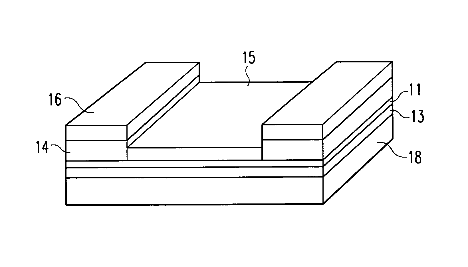
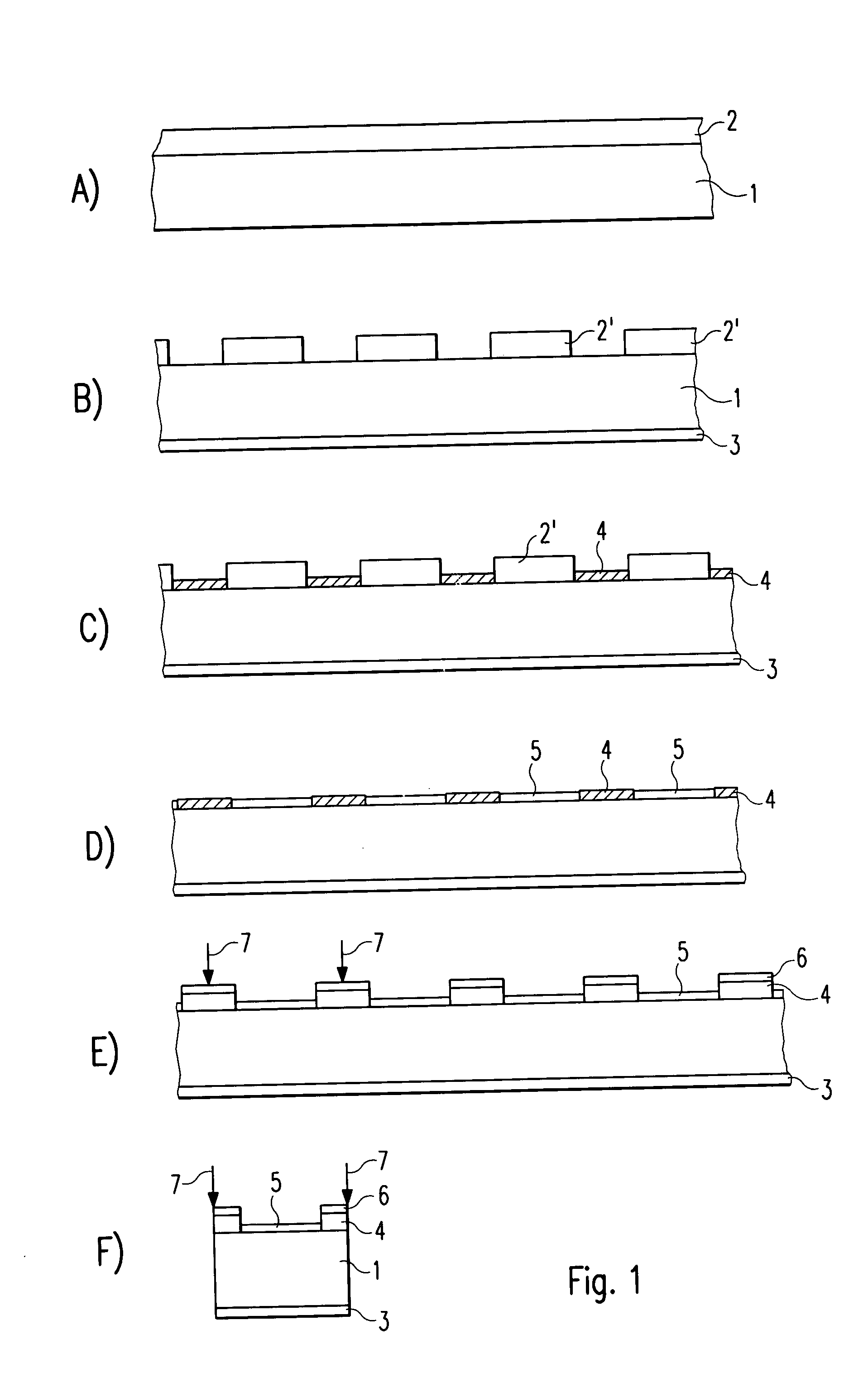
[0017] According to FIG. 1A), in the first process step, a blank rectangular metal sheet 1 consisting of a metallic resistor alloy is coated with a photoresist layer 2 which can be illuminated, in the manner conventionally used in photolithography, through a photomask (not shown). The metal sheet 1, in practical cases, can have a useful surface area of, for example, approximately 300×400 mm, and a thickness between 0.1 and 1 mm. It is preferably made of one of the proven resistor alloys based on Cu such as CuMn12Ni or a similar material.

[0018] In the next step, according to FIG. 1B), again in a manner which in itself is known, the photolithographic structure of the photoresist layer 2 is formed by partial removal. This structure, which serves as cover mask, consists of a multitude of parallel strips 2′ which extend over the entire width or length of the top surface (in the drawing) of the metal sheet 1, or at least of the surface area to be used; as a rule, the strips have the same...


PUM


Abstract

In the manufacture of low-impedance electrical resistors made of a metal sheet or a film consisting of a metallic resistance alloy, a metal forming the connection contacts of the resistors is electroplated onto a multitude of photolithographically defined parallel strips, which extend, at regular mutual intervals, over the entire metal sheet or film surface. To separate the resistors, the electroplated metal piece is sawed longitudinally into cutting planes, which extend perpendicularly with respect to each other, and with respect to the metal sheet, where, in each case, the cutting planes of one group divide one of the connection contact strips in its longitudinal direction.

Description

DESCRIPTION OF THE BACKGROUND OF THE INVENTION [0001] 1. Field of the Invention [0002] The invention relates to a low-impedance electrical resistor and a process for its manufacture according to the preamble of the independent claims. In particular, the resistors are low-impedance precision resistors for current measurement purposes of the SMD or chip construction type. [0003] 2. Background Art [0004] In a process for the manufacture of SMD measurement resistors with resistance values in the milliohm range, a laminate is first formed from a copper metal sheet which serves as substrate and from a film consisting of a Cu-based resistor alloy and a heat-conducting adhesive located between them. On the free top side of the alloy film, connection contact areas for the individual resistors are then photolithographically defined, coated with copper by an electroplating process and covered with nickel. After the electroplating metallization, the structure itself of the resistors and their c...

Claims


Application Information

Patent Timeline
IPC IPC(8): H01C1/142H01C17/00H01C17/28
CPCH01C1/142H01C17/281H01C17/006H01C17/003
Inventor HETZLER, ULLRICH U.
Owner ISABELLENHUTTE HEUSLER
Why Eureka
Try Eureka