

Method for fabricating liquid crystal display device
- Summary
- Abstract
- Description
- Claims
- Application Information
AI Technical Summary
Benefits of technology
Problems solved by technology
Method used
Image

Examples
first embodiment
[0047]FIG. 8 is a plan view illustrating an IPS mode LCD device according to the present invention. FIG. 9A to FIG. 9E are cross-sectional views illustrating the fabrication process of an IPS mode LCD device, taken along line I-I′ of FIG. 8. FIG. 10 is a cross-sectional view illustrating an ion beam irradiation device according to the present invention. FIG. 11 is a schematic view illustrating a light irradiation device according to the present invention.
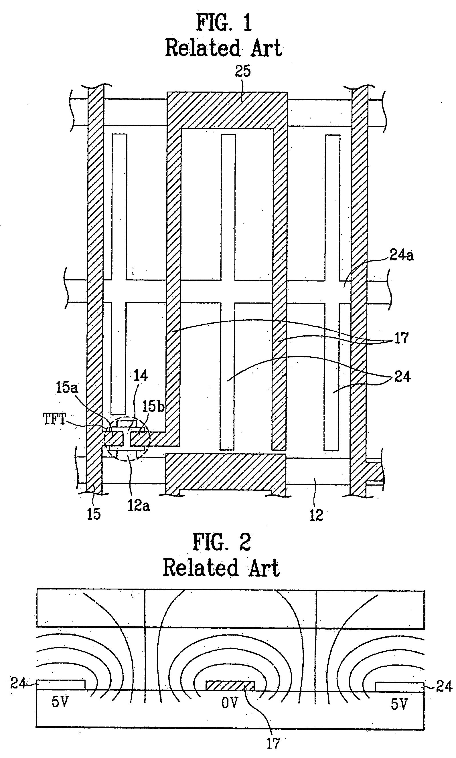
[0048] As shown in FIG. 8, the LCD device according to the first embodiment of the present invention includes a gate line 112, a data line 115, a common line 124a, a thin film transistor TFT, a common electrode 124, a pixel electrode 117, and a storage electrode 125. The gate and data lines 112 and 115 are formed on a substrate substantially perpendicular to each other to define a pixel region. The common line 124a is substantially parallel to the gate line 112 within the pixel region, and the thin film transistor TFT is formed at a...
second embodiment
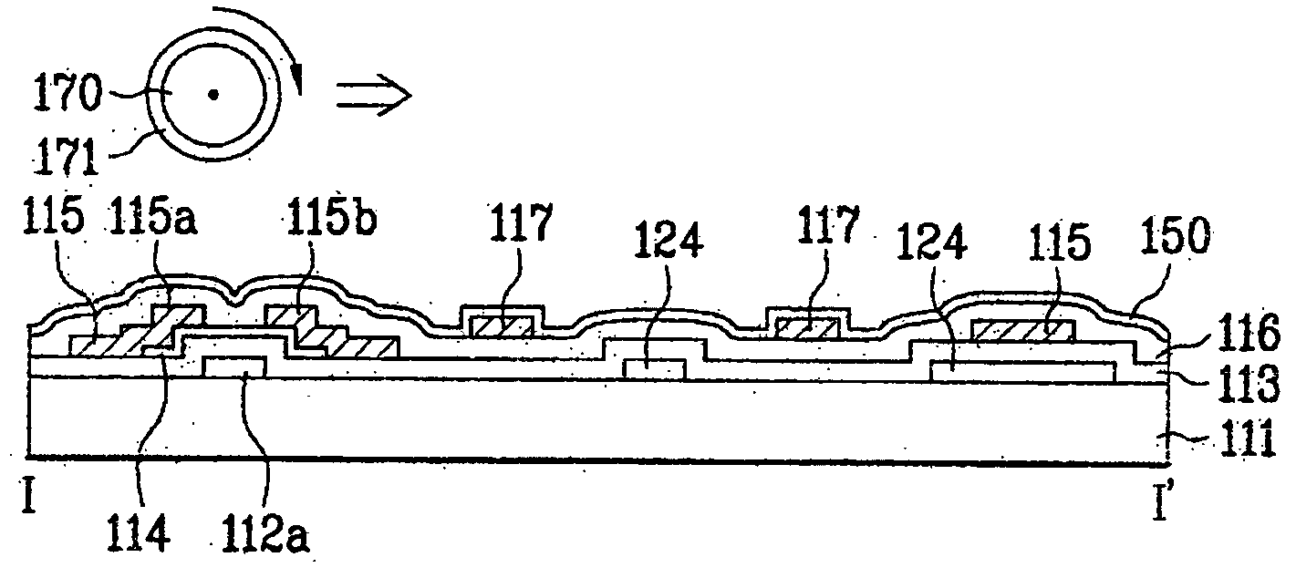
[0066]FIG. 14 is a cross-sectional view illustrating an IPS mode LCD device, wherein a pixel electrode and a common electrode are formed of transparent conductive layers, according to the present invention. That is, a gate line (not shown) having a gate electrode 112a is formed on a substrate, and a gate insulating layer 113 is formed on an entire surface of the substrate including the gate electrode 112a. Then, a semiconductor layer 114 is formed on the gate insulating layer 113 above the gate electrode 112a. Also, a data line is formed substantially perpendicular to the gate line. Simultaneously, source and drain electrodes 115a and 115b are formed at both sides of the semiconductor layer 114. Thereafter, a passivation layer 116 having a contact hole in the drain electrode 115 is formed on an entire surface of the substrate including the source and drain electrodes 115 and 115b. Then, a common electrode 124 and a pixel electrode 117 are formed of a transparent conductive layer in ...
third embodiment
[0067] In a method for fabricating the IPS mode LCD device using three masks, the rubbing process and the orientation direction alignment process (using, for example, ion beam irradiation, light irradiation or plasma irradiation) are performed together because there is a step portion at a contact portion between the pixel electrode and the drain electrode of the thin film transistor, thereby preventing defective orientation. This embodiment will be described in detail with reference to FIG. 15A to FIG. 15I, which are cross-sectional views illustrating the fabrication process of an LCD device according to the present invention using three masks along the line II-II′ of FIG. 8.
[0068] As shown in FIG. 15A, a low-resistance metal layer having low specific resistance is formed on a lower substrate 111 to prevent signal delay. The metal layer is patterned using photolithography to form a gate line and a gate electrode 112a of a thin film transistor, the gate electrode 112a diverged from t...
PUM
 Abstract
Description
Claims
Application Information