Optical head apparatus and optical information processing apparatus

a head apparatus and head technology, applied in the field of optical head apparatus and optical information processing apparatus, can solve the problems of increasing the effective diameter of the necessary optical element, requiring a far greater positive power, and unable to obtain sufficient characteristics and accuracy, so as to reduce the length of the optical path of the entire optical system, the effect of reducing the length of the optical path and ensuring the working distan

Inactive Publication Date: 2005-03-03
SONY CORP
View PDF6 Cites 5 Cited by
  • Summary
  • Abstract
  • Description
  • Claims
  • Application Information

AI Technical Summary

Benefits of technology

[0014] In the present invention, since use is made of the diffraction action of the hologram surface, larger power can be obtained, and the surface or surfaces of the optical element located on the optical-recording-medium side need not be arranged excessively close to the optical recording medium, whereby the above-mentioned working distance can be sufficiently ensured. In addition, a reflective element need not be arranged on the optical path.
[0015] According to the present invention, it is possible to reduce the optical path length of the entire optical system and promote miniaturization of apparatuses. It is also possible to realize reductions in the number of component parts and cost reductions by omitting a mirror for changing an optical path.
[0016] The above-mentioned optical elements can be reduced in the number of the component parts and the costs by adopting a construction in which a first optical device including a surface having negative power and a second optical device including a surface having positive power are combined with each other, or a construction which uses only one optical element constructed so that one surface has negative power and another surface has positive power. Accordingly, the optical elements are suited to miniaturization applications and high accuracy applications.
[0017] In the case where the hologram surface is formed as a composite surface on which a hologram pattern is formed on an aspherical surface, spherical aberration can be made small, whereby good optical characteristics can be obtained. In the case where the hologram surface is formed as a surface on which a hologram pattern is formed on a plane surface, the hologram having the desired diffraction action can be easily and highly accurately formed on a surface having no power.
[0018] In addition, since the hologram pattern is formed on the hologram surface in a region which determines the necessary numerical aperture, it is possible to control the numerical aperture without using an aperture.

Problems solved by technology

To realize the above-mentioned optical system, it is necessary to make the optical path length as short as possible, and this leads to the difficulty that in any conventional form of construction, sufficient characteristics and accuracy are difficult to obtain.
As a result, far greater positive power is required for the optical element, so that the necessary effective diameter necessarily becomes large.
If large power is to be obtained in each of the optical elements having positive power and negative power, the curvatures of their constituent surfaces need to be made large, i.e., surfaces having smaller radii of curvature become necessary, so that the lenses become thick and cannot be accommodated within the necessary optical path length or problems will occur in lens fabrication (difficulty in manufacturing molds, degradation of transfer of molding shapes, and the like).
In addition, as a problem associated with optical design, there may be, for example, the disadvantage that although a radius of curvature which is approximately not greater than an effective radius is necessary, a solution for a lens cannot be found.

Method used


Image

  • Optical head apparatus and optical information processing apparatus
  • Optical head apparatus and optical information processing apparatus
  • Optical head apparatus and optical information processing apparatus

Examples


embodiment 1

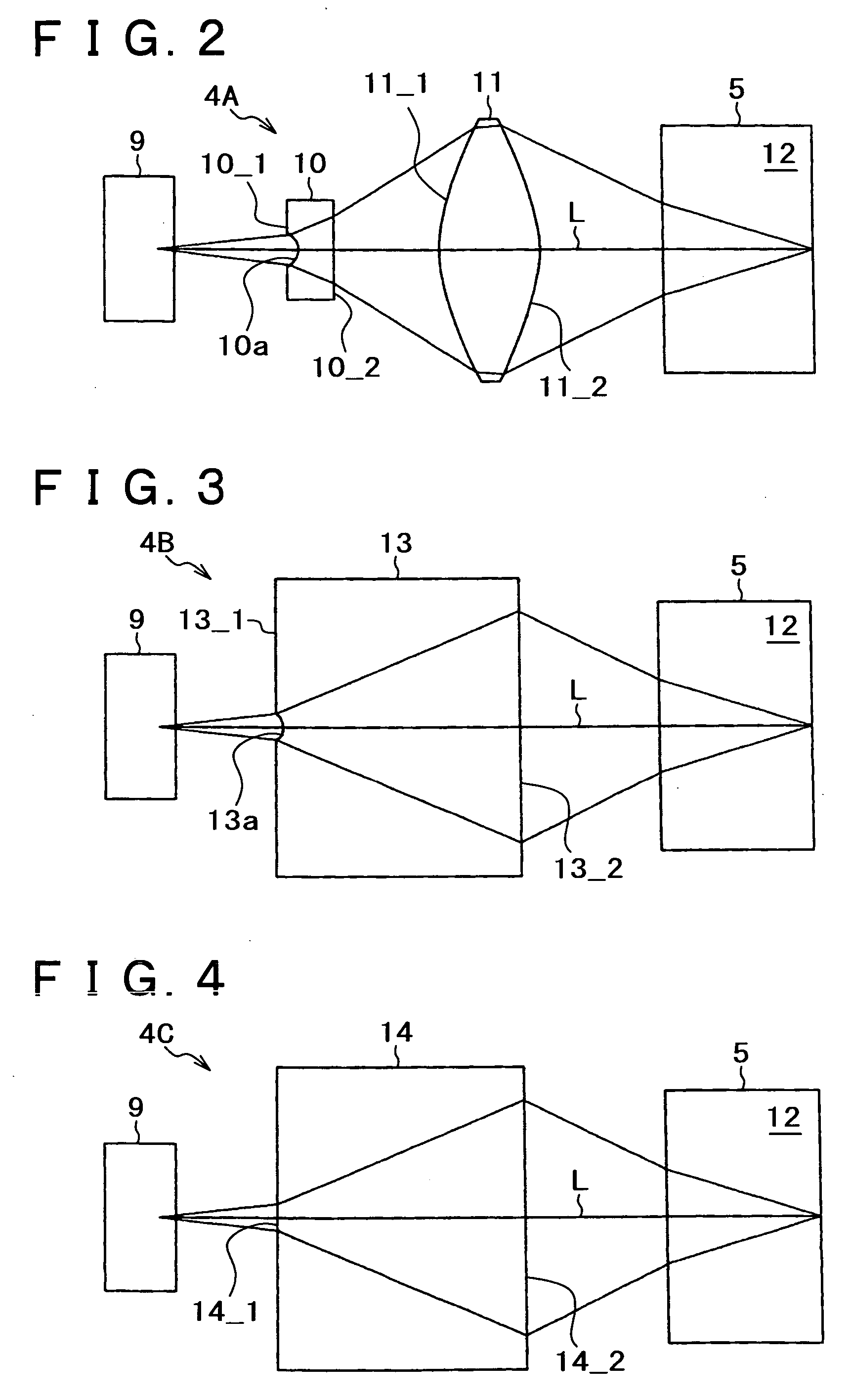
[0042]FIG. 2 shows the essential portion of an optical system associated with the above-mentioned form (I), and in FIG. 2, “L” denotes its optical axis.

[0043] In an optical system 4A shown in this embodiment, a composite element (a so-called laser coupler) of a laser diode and a photodetector is used as a light-emitting / receiving element (or a light-transmitting / receiving element) 9, and light exiting from the composite element, after having been transmitted through a coupling lens 10, is irradiated onto an optical disk 12 (part of which is shown in FIG. 2) via an objective lens 11.

[0044] The coupling lens 10 disposed near the light-emitting / receiving element 9 has negative power as a whole. In this embodiment, a concave surface 10a is formed on a first surface 10_1 opposed to the light-emitting / receiving element 9, and a second surface 10_2 on the side of an optical disk 12 is formed as a plane surface. Incidentally, the concave surface 10a is formed as an aspherical surface havi...

embodiment 2

[0049]FIG. 3 shows the essential portion of an optical system associated with the above-mentioned form (II), and “L” denotes its optical axis.

[0050] In an optical system 4B shown in this embodiment, the light-emitting / receiving element 9 which is the same as that of Embodiment 1 is used, and light exiting therefrom, after having been transmitted through a hologram element 13, is irradiated onto the optical disk 12.

[0051] In the hologram element 13, a first surface 13_1 opposed to the light-emitting / receiving element 9 has negative power, and a concave surface 13a is formed as an aspherical surface of negative curvature. A second surface 13_2 opposed to the optical disk 12 is formed as a hologram surface having positive power. Namely, in this embodiment, positive power is obtained only from the surface on which the hologram pattern is formed on a plane surface, whereby the optical path length of the entire system can be made short.

[0052] Since the first surface having negative pow...

embodiment 3

[0053]FIG. 4 shows the essential portion of an optical system associated with the above-mentioned form (II), and in FIG. 4, “L” denotes its optical axis.

[0054] An optical system 4C shown in this embodiment differs from the optical system 4B shown in Embodiment 2 in that both the first and second surfaces of its hologram element are formed as hologram surfaces.

[0055] Namely, light exiting from the light-emitting / receiving element 9 is irradiated onto the optical disk 12 after having been transmitted through a hologram element 14, and in the hologram element 14, a first surface 14_1 opposed to the light-emitting / receiving element 9 is formed as a hologram surface having negative power, and a second surface 14_2 opposed to the optical disk 12 is formed as a hologram surface having positive power.

[0056] In this embodiment as well, it is advantageous in terms of accuracy and the number of component parts that the first surface having negative power and the second surface having positi...


PUM

PropertyMeasurementUnit
heightaaaaaaaaaa
poweraaaaaaaaaa
optical path lengthaaaaaaaaaa

Abstract

To reduce the optical path length of the entire optical system in a reproduction or recording optical system of an optical recording medium, and promote miniaturization and reductions in costs of apparatuses. An optical head apparatus has an optical system an including a light source and a translucent optical element and irradiates light exiting from the light source, after having been transmitted through the optical element, onto the optical recoding medium. The optical element has a surface or surfaces having negative power on the light-source side and a surface or surfaces having positive power on the optical-recording-medium side. In order to increase the power of the surface or surfaces, one or more of these surfaces are formed as a hologram surface on which a concentric hologram pattern is formed.

Description

CROSS REFERENCE TO RELATED APPLICATION [0001] The present document is based on Japanese Priority Document JP2003-291310, filed in the Japanese Patent Office on Aug. 11, 2003, the entire contents of which being incorporated herein by reference. BACKGROUND OF THE INVENTION [0002] 1. Technical Field [0003] The present invention relates to a technique for reducing an optical path length in an optical system for performing reading or recording of information by making use of light irradiation onto an optical recording medium. [0004] 2. Description of Related Art [0005] An optical head apparatus (such as an optical pickup apparatus) to be used for the reproduction and recording of information associated with an optical disk is provided with, for example, a light source such as a laser diode, lens elements (such as a collimator lens and a coupling lens) which convert light scattered from the light source into an approximately parallel light beam, and an objective lens which condenses the l...

Claims


Application Information

Patent Timeline
Patent Type & Authority Applications(United States)
IPC IPC(8): G11B7/00G11B7/12G11B7/123G11B7/135G11B7/1353G11B7/1378G11B7/139G11B7/1392
CPCG11B7/1205G11B7/1353G11B7/13922G11B7/139G11B7/1378G11B7/123
Inventor ABE, TSUGUHIRO
Owner SONY CORP
Why Eureka
Try Eureka