Method for ultra low-K dielectric deposition

Inactive Publication Date: 2005-03-03
TAIWAN SEMICON MFG CO LTD
View PDF8 Cites 44 Cited by
  • Summary
  • Abstract
  • Description
  • Claims
  • Application Information

AI Technical Summary

Problems solved by technology

Not surprisingly, these material changes have required changes in the processing methods.
For example, because of the difficulty of etching copper without also causing unacceptable damage to the dielectric material, the technique of forming the metal interconnect lines has experienced significant changes.
Unfortunately, problems arise in the depositing of this low-K dielectric materi

Method used


Image

  • Method for ultra low-K dielectric deposition
  • Method for ultra low-K dielectric deposition
  • Method for ultra low-K dielectric deposition

Examples


Embodiment Construction

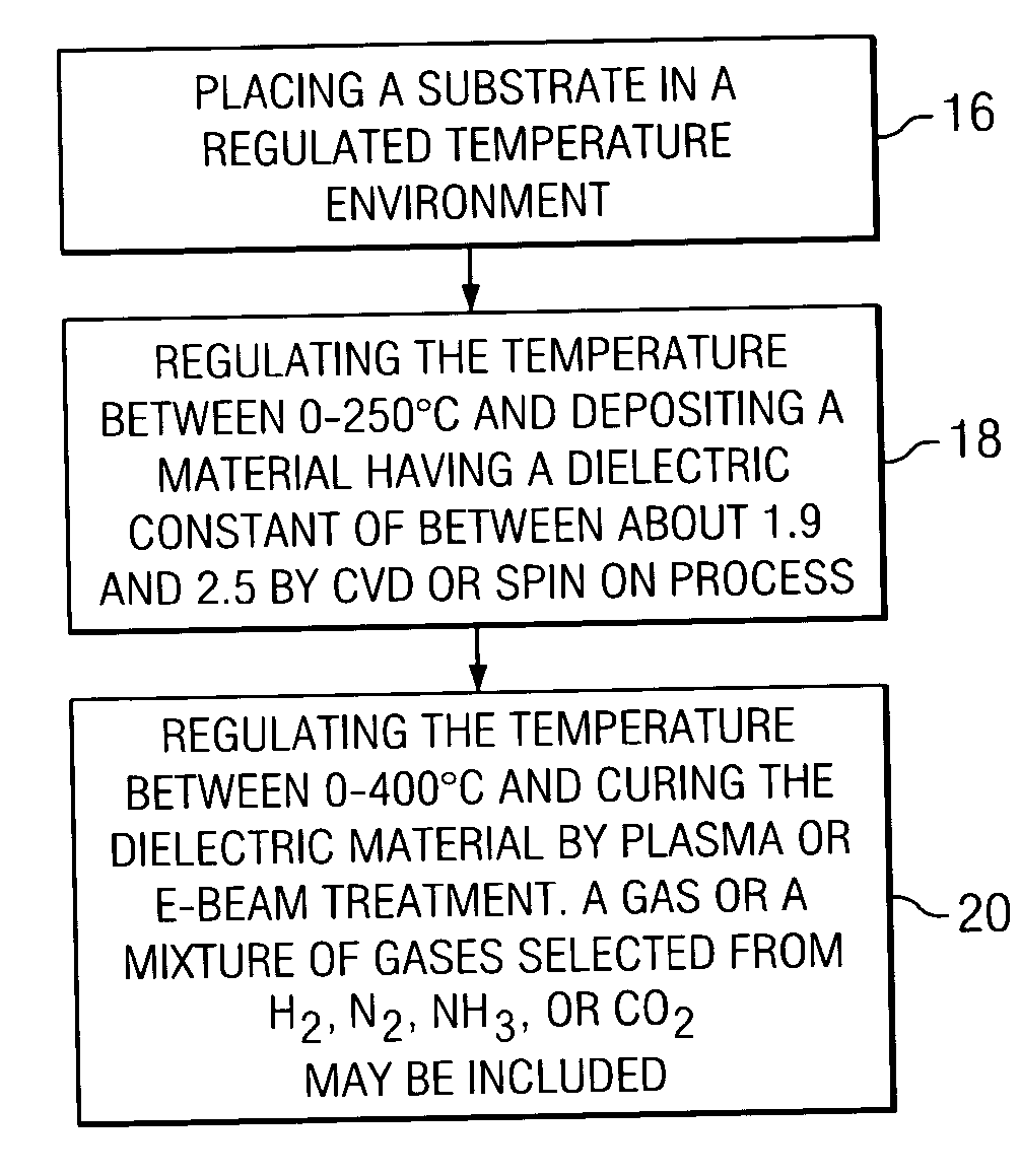
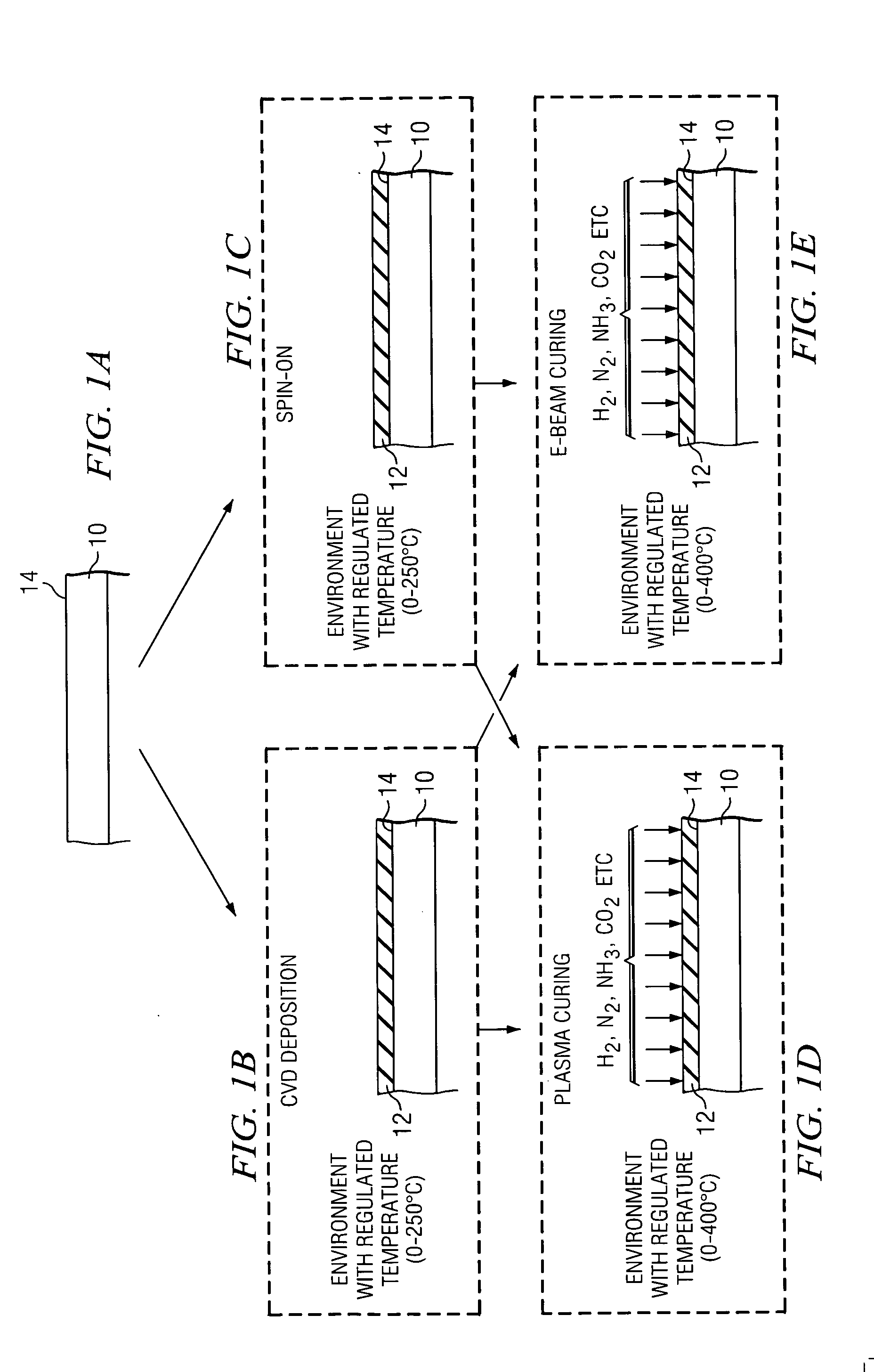
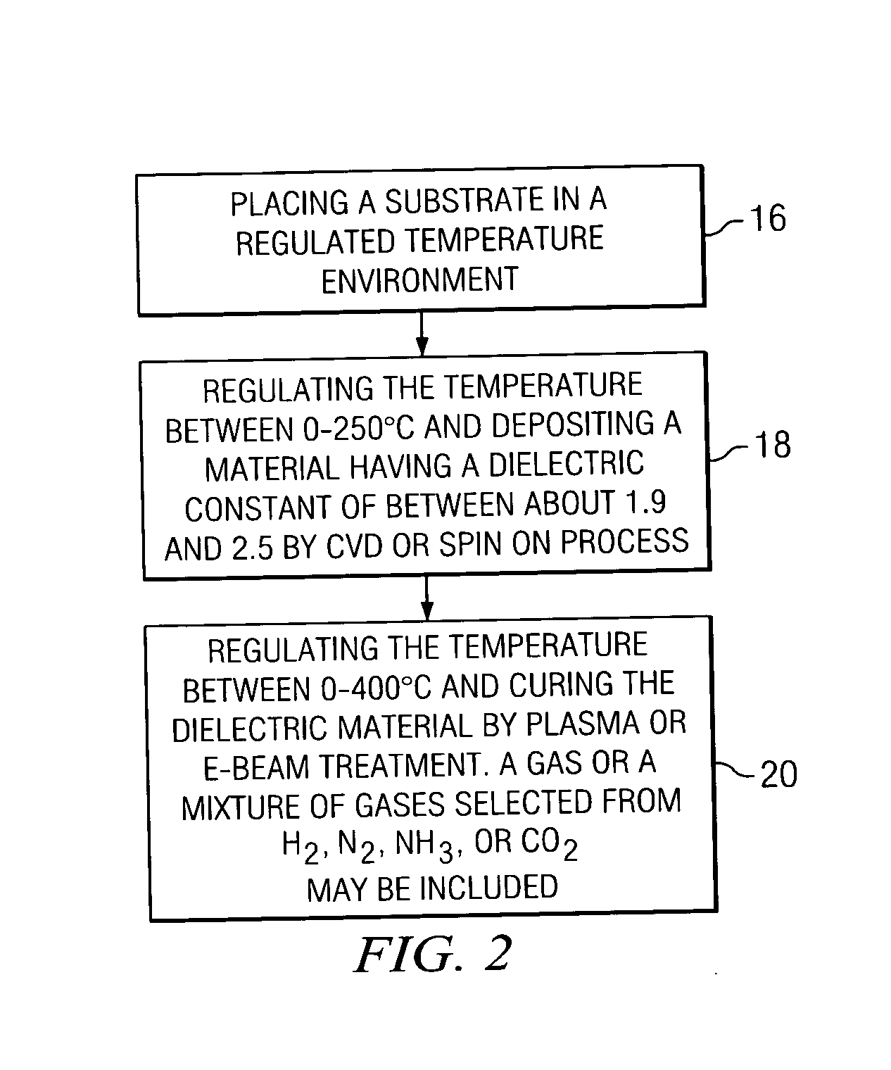
[0009] Referring now to FIG. 1A, there is shown a typical substrate 10 used in the manufacture of semiconductor devices. According to the present invention, the substrate is placed in a controlled environment where the temperature can be maintained at between about 0° C. and about 250° C. An ultra low-K dielectric material 12 is then deposited on the top surface 14 of the substrate by a CVD (chemical vapor deposition) process or a spin-on process at these low temperatures and as shown in FIGS. 1B and 1C, respectively. The term “ultra low-K” is used herein to mean a dielectric constant of between 1.9 and 2.5. Suitable examples of ultra low-K materials may include the SiLK™ manufactured by the Dow Chemical Company of Midland, Michigan, or an “organosilcate” material such as ORION™ manufactured by the Trikon company of Newport in the United Kingdom, porous MSQ films and various florocarbonated silicon films. For a material such as ORION™ a precursor such as methysilane (SiH3CH3) and hy...


PUM


Abstract

The present invention provides a method of forming a semiconductor structure having an ultra low-K dielectric material that adheres well to the substrate. The method includes depositing a low-K material on the top surface of a substrate at a low temperature of no more than 250° by a CVD or spin-on process. The dielectric material is then cured by placing the substrate with the dielectric film in an environment where the temperature is regulated at about 400° or less as the dielectric film is being subjected to a plasma treatment or an E-beam treatment or UV treatment. The environment may further include one or more gases or a mixture of gases selected from the group consisting of H2, N2, NH3, CO2, all hydride gases and a mixture of these gases.

Description

TECHNICAL FIELD [0001] The present invention relates generally to the deposition of dielectric materials used with a Damascene process for depositing copper interconnect lines, and more particularly to a method of depositing ultra low-K materials between the metal conductors deposited by the Damascene process. BACKGROUND [0002] As is well known by those skilled in the art, a continuing goal in manufacturing and production of semiconductors is a reduction in size of components and circuits with the concurrent result of an increase in the number of circuits and / or circuit elements such as transistors, capacitors, etc., on a single semiconductor device. This relentless and successful reduction in size of the circuit elements has also required reduction in the size of the conductive lines connecting devices and circuits. However, as the conducting lines are designed to be smaller and smaller, the resistance of the interconnects increases. Further, as the number of dielectric layers incr...

Claims


Application Information

Patent Timeline
IPC IPC(8): H01L21/312H01L21/768
CPCH01L21/312H01L21/7682H01L21/3121H01L21/02271H01L21/02282H01L21/02126H01L21/0234H01L21/02351H01L21/02348
Inventor KO, CHUNG-CHILU, YUNG-CHENGBAO, TIEN-ICHANG, HUI-LINJANG, SYUN-MING
Owner TAIWAN SEMICON MFG CO LTD
Why Eureka
Try Eureka