

Electro-optical device and electronic apparatus
a technology of optical devices and electronic devices, applied in the direction of optics, identification means, instruments, etc., can solve the problems of frequent generation of crosstalk, image signal interference between pixel rows, and possible causes of image display faults, etc., to achieve significant reduction of parasitic capacitance, and relatively large parasitic capacitance reduction
- Summary
- Abstract
- Description
- Claims
- Application Information
AI Technical Summary
Benefits of technology
Problems solved by technology
Method used
Image

Examples
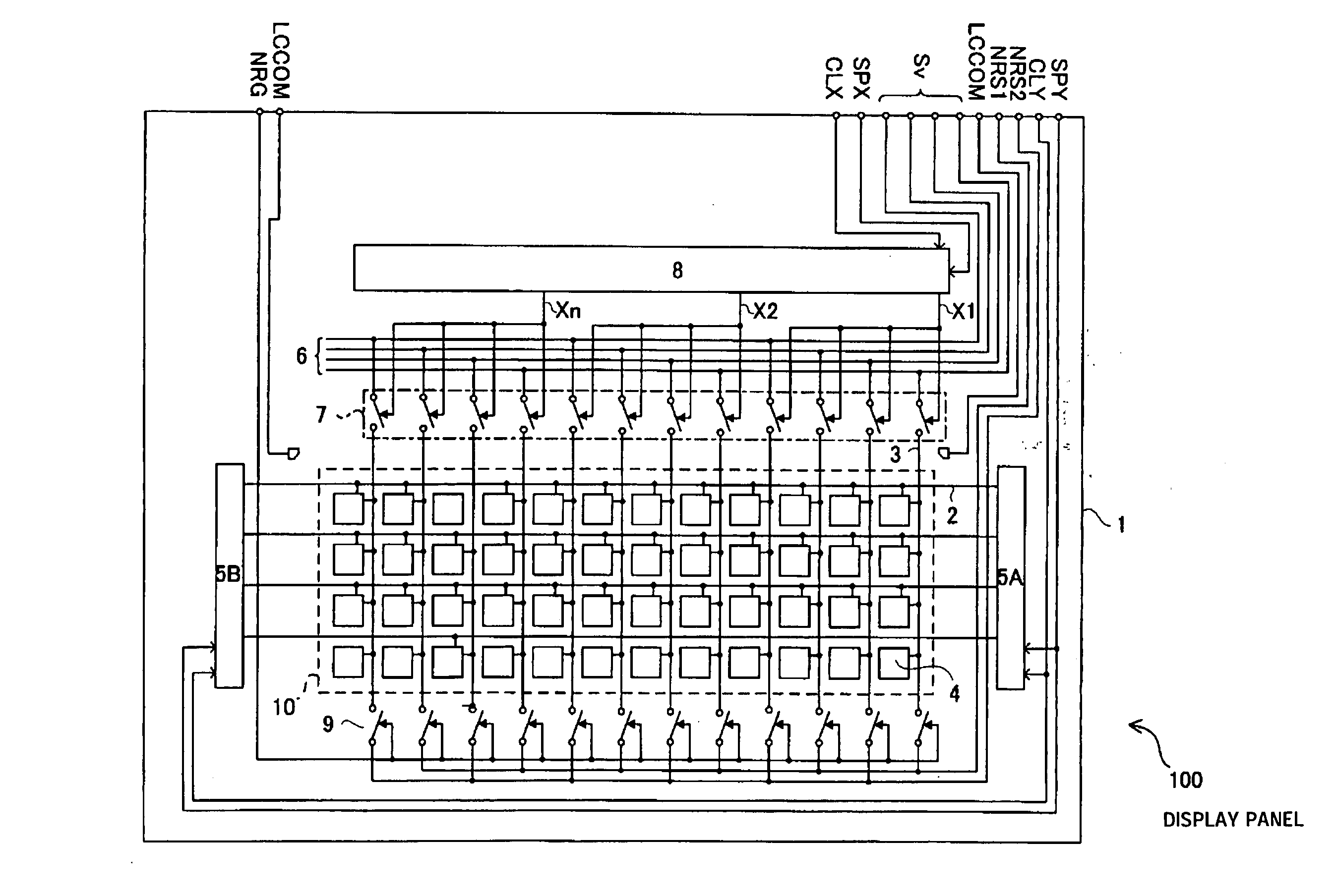
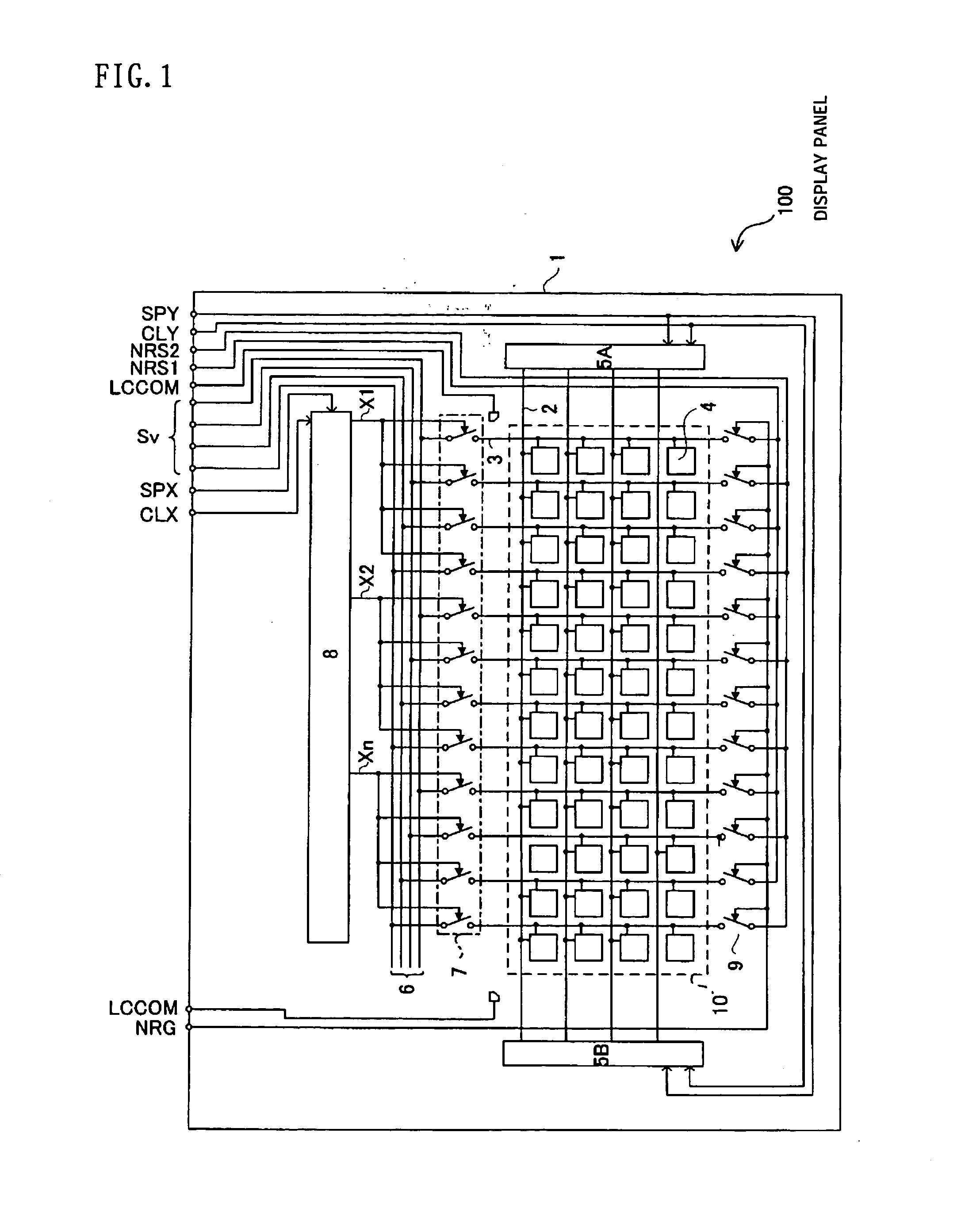
first embodiment
[0083]FIG. 8 illustrates a first modification of the sampling circuit in the first exemplary embodiment. In the first exemplary embodiment, the source wiring lines of the sampling TFTs 71 in each group are arranged adjacent to each other with the boundary R interposed therebetween. However, in the present modification, the drain wiring lines of the sampling TFTs 71 in each group are arranged adjacent to each other with the boundary R interposed therebetween. For example, according to the modification illustrated in FIG. 8, each group of the sampling TFTs 71 is constituted using only the TFTs 71A, except that the TFT 71B is arranged at the left end of each group. In addition, the TFT 71A is arranged at the left end and the TFT 71B is arranged at the right end, with the boundary R interposed therebetween (in the first embodiment, the TFT 71B is arranged at the right end of the group and the TFT 71B is arranged at the left end and the TFT 71A is arranged at the right end with the bound...
second embodiment
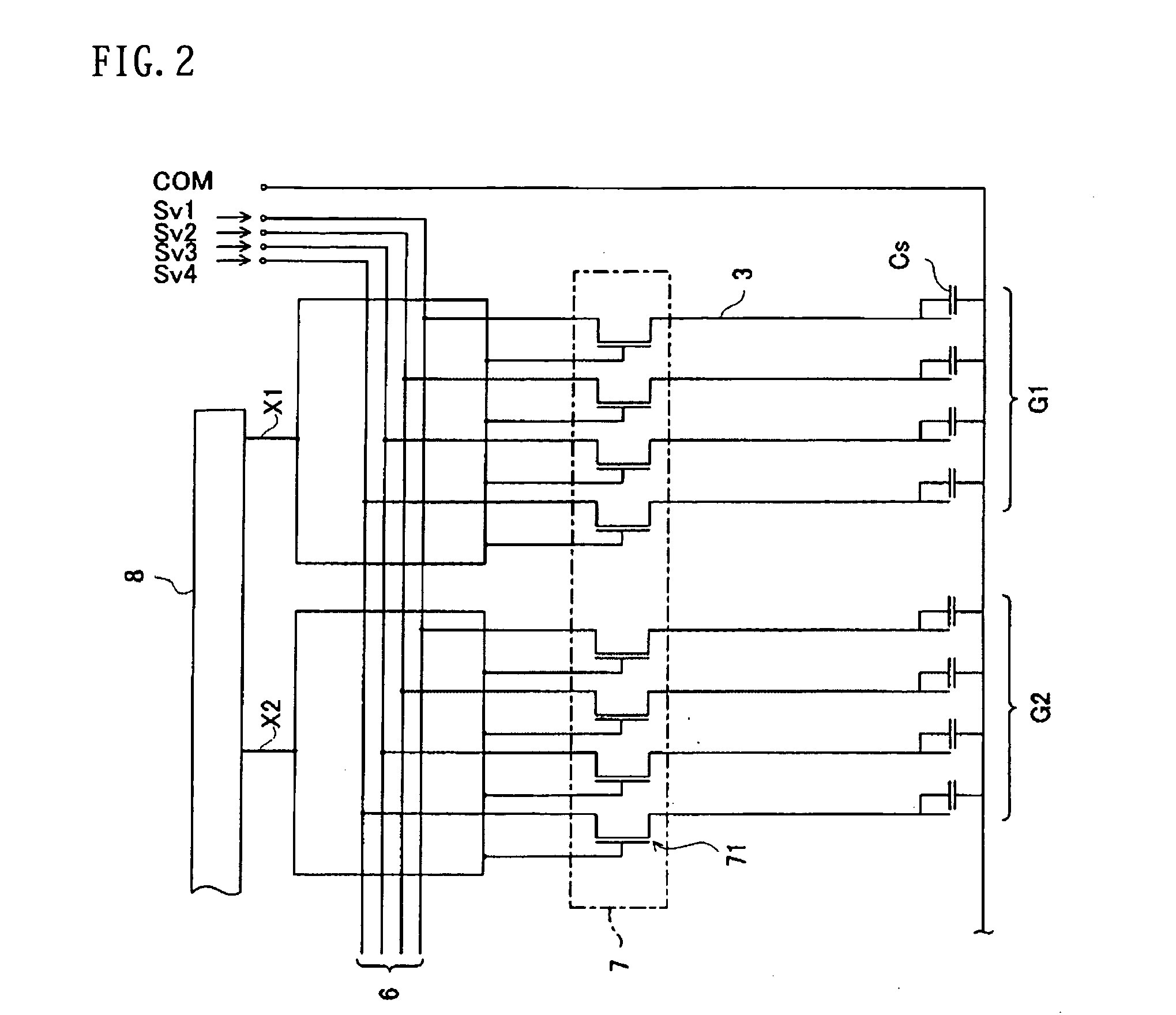
[0087]FIG. 10 illustrates the configuration of the sampling circuit according to the In the sampling circuit 17, TFTs (here, TFTs 71A) having the same structure are arranged parallel to each other. A gap W1 between the TFTs 71A adjacent to each other with a boundary R of the groups interposed therebetween is larger than a gap W2 between the TFTs 71A adjacent to each other in the groups.
[0088] In this case, the capacitance between groups (FIG. 7: capacitance C22) is reduced by the gap W1. Accordingly, the variation of the voltage of the data line 3 and the pixel portion 4 caused by the capacitance C22 between groups is reduced such that the image display can be performed without deteriorating the image quality due to the ghost images.
[0089] Moreover, the component of the parasitic capacitance having a large influence on the image quality is reduced, such that the wiring line pitch of the sampling TFT 71, which is in a trade-off relation together with the parasitic capacitance, can ...
third embodiment
[0093] Next, a third exemplary embodiment will be described with reference to FIGS. 12 and 13. The main configuration of an electro-optical device is the same as in the first exemplary embodiment except for the layout of a sampling circuit. Accordingly, the same constituent elements as the first exemplary embodiment are denoted by the same reference numerals and the description thereof will be omitted.
[0094]FIG. 12 illustrates the configuration of the sampling circuit according to the third embodiment. In the sampling circuit 27, TFTs (here, TFTs 71A) having the same structure are arranged parallel to each other. However, only a TFT 71C that is one of the sampling TFTs 71 adjacent to each other with the boundary R of the group interposed therebetween is displaced by a distance L in the direction in which the data line 3 extends.
[0095] In this case, the capacitance between groups (FIG. 7: capacitance C22) is reduced according to the distance L, the shift amount of the TFT 71C. Acco...
PUM
| Property | Measurement | Unit |
|---|---|---|
| length | aaaaa | aaaaa |
| parasitic capacitance | aaaaa | aaaaa |
| area | aaaaa | aaaaa |
Abstract
Description
Claims
Application Information