Local SONOS-type nonvolatile memory device and method of manufacturing the same

a nonvolatile memory and silicon oxide technology, applied in the direction of semiconductor devices, electrical devices, transistors, etc., can solve the problems of difficult integral formation of stack sonos-type cells, high power dissipation, and more difficult scaling down and pattern cells, so as to achieve the effect of minimizing the overlap length, great scaling down, and reducing the length of control gates and ono layers

Inactive Publication Date: 2005-03-10
SAMSUNG ELECTRONICS CO LTD
View PDF4 Cites 85 Cited by
  • Summary
  • Abstract
  • Description
  • Claims
  • Application Information

AI Technical Summary

Benefits of technology

[0029] In one embodiment, the forming of the ONO layer and the conductive layer in a self-aligned manner between the pair of insulating spacers comprises: forming an ONO layer on the pair of insulating spacers; patterning the ONO layer such that the ONO layer remains only between the pair of insulating spacers; forming a conductive layer on the patterned ONO layer; and patterning the conductive layer such that the conductive layer remains only between the p

Problems solved by technology

However, as the integration density of semiconductor devices increases, it becomes more difficult to scale down and pattern cells.
Because of the high threshold voltage, power dissipation is high and it is difficult to integrally form the stack SONOS-type cell along with a typical logic device having a low initial threshold voltage in a single chip.
However, in the local

Method used


Image

  • Local SONOS-type nonvolatile memory device and method of manufacturing the same
  • Local SONOS-type nonvolatile memory device and method of manufacturing the same
  • Local SONOS-type nonvolatile memory device and method of manufacturing the same

Examples


Embodiment Construction

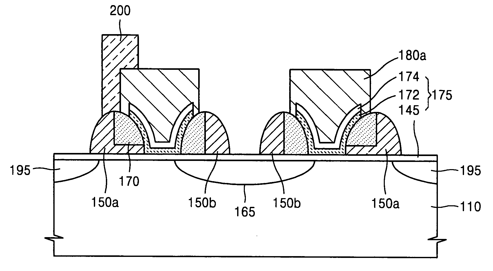
[0039] In the drawings, the forms of elements are exaggerated for clarity. FIGS. 4 through 14 are cross-sectional views illustrating a method of manufacturing a local SONOS-type nonvolatile memory device according to an embodiment of the present invention.

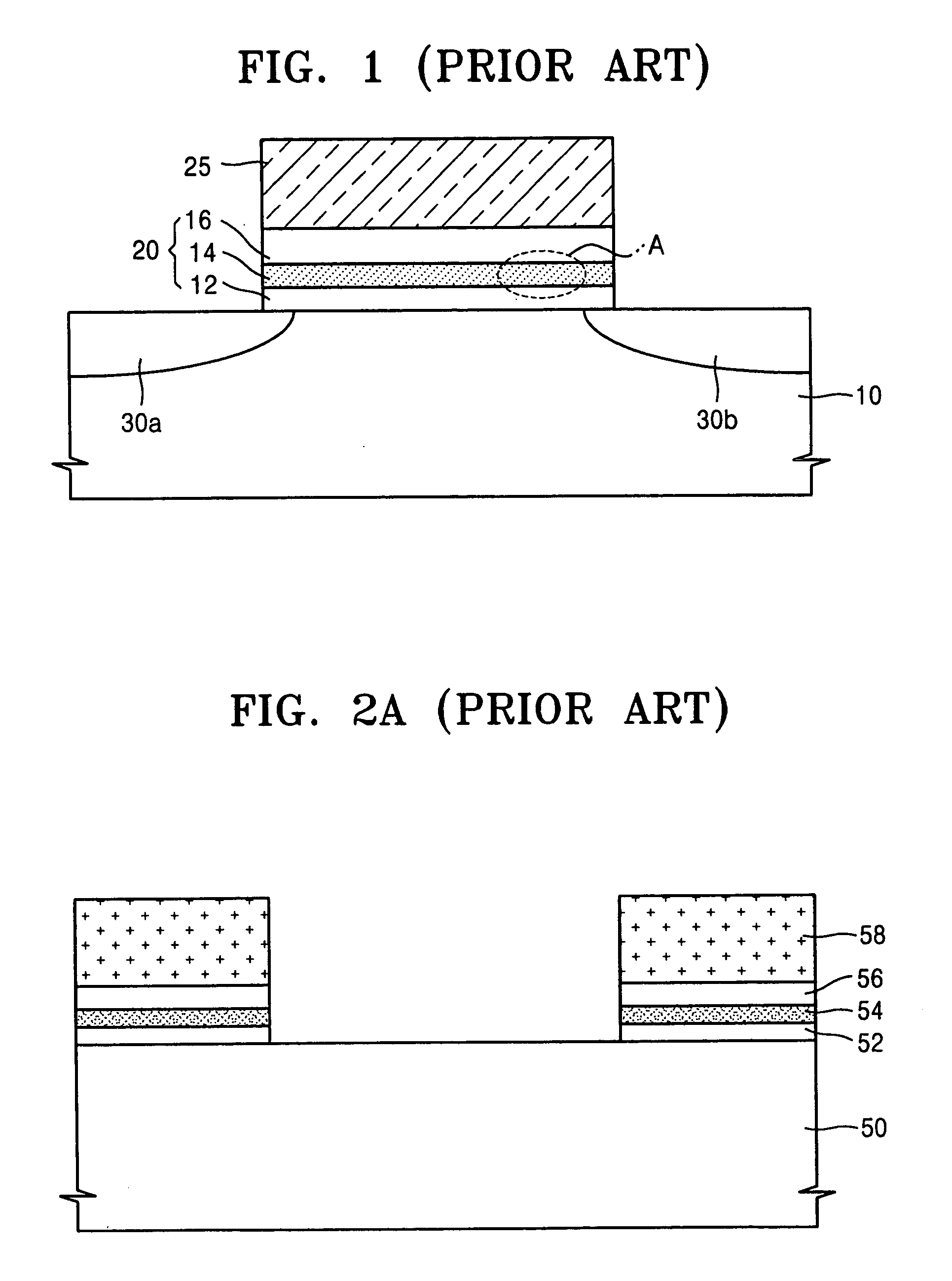
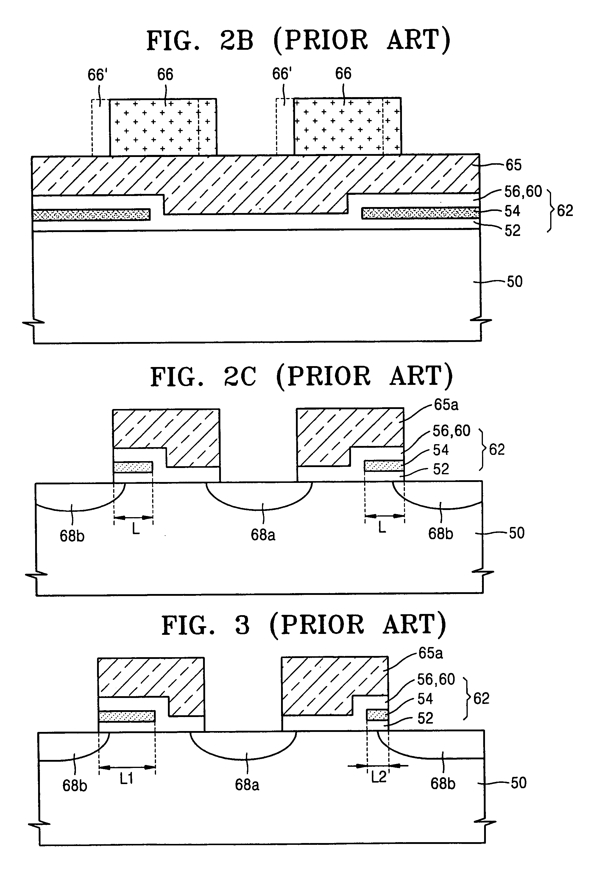
[0040] Referring to FIG. 4, insulating patterns 130 are formed on a silicon substrate 110 and separated by an opening 115. An insulating pattern 130 can be comprised of two stacked layers, which have a high etch selectivity with respect to each other. In one embodiment, the insulating pattern 130 is comprised of an oxide layer 120 and a nitride layer 125, which are sequentially stacked. To form the insulating pattern 130, the oxide layer 120 and the nitride layer 125 are deposited on the entire surface of the silicon substrate 110 and patterned by a photolithography process using a first photoresist pattern (not shown), which is formed to define the opening 115. Thereafter, the first photoresist pattern is removed by ashing and st...


PUM


Abstract

Provided are a local SONOS-type memory device and a method of manufacturing the same. The device includes a gate oxide layer formed on a silicon substrate; a conductive spacer and a dummy spacer, which are formed on the gate oxide layer and separated apart from each other, the conductive spacer and the dummy spacer having round surfaces that face outward; a pair of insulating spacers formed on a sidewall of the conductive spacer and a sidewall of the dummy spacer which face each other; an ONO layer formed in a self-aligned manner between the pair of insulating spacers; a conductive layer formed on the ONO layer in a self-aligned manner between the pair of insulating spacers; and source and drain regions formed in the silicon substrate outside the conductive spacer and the dummy spacer.

Description

[0001] This application claims priority to Korean Patent Application No. 2003-63355, filed on Sep. 9, 2003, in the Korean Intellectual Property Office, the contents of which are hereby incorporated by reference in their entirety as fully set forth herein. BACKGROUND OF THE INVENTION [0002] 1. Field of the Invention [0003] The present invention relates to a local silicon-oxide-nitride-oxide-silicon (SONOS)-type nonvolatile memory device and a method of manufacturing the same. More particularly, the present invention relates to a local SONOS-type nonvolatile memory device in which an oxide-nitride-oxide (ONO) layer and a control gate are formed in a self-aligned manner, and a method of manufacturing the same. [0004] 2. Description of the Related Art [0005] A nonvolatile memory device can electrically erase and store data and retain data even if power supply is interrupted. The nonvolatile memory device has increasingly been applied in various fields such as mobile communication system...

Claims


Application Information

Patent Timeline
IPC IPC(8): H01L21/28H01L21/336H01L21/8246H01L21/8247H01L27/115H01L29/788H01L29/792
CPCH01L21/28282H01L27/115H01L29/792H01L29/66833H01L27/11568H01L29/40117H10B69/00H10B43/30
Inventor CHOI, YONG-SUKYOON, SEUNG-BEOMKIM, SEONG-GYUN
Owner SAMSUNG ELECTRONICS CO LTD
Why Eureka
Try Eureka