Method for suppressing boron penetration by implantation in P+ MOSFETS

a technology of boron penetration and implantation, which is applied in the direction of semiconductor devices, basic electric elements, electrical appliances, etc., can solve the problems of reduced channel length, unintended and undesirable leakage current in the channel region, and undesired shi

Inactive Publication Date: 2005-03-10
MACRONIX INT CO LTD
View PDF11 Cites 11 Cited by
  • Summary
  • Abstract
  • Description
  • Claims
  • Application Information

AI Technical Summary

Benefits of technology

[0006] Also in accordance with the present invention, there is provided a method for suppressing boron penetration of a gate oxide during the manufacture of an integrated circuit that includes providing a substrate, forming a plurality of isolation regions, forming a layer of gate oxide over the substrate, depositing a layer of silicon material over the layer of gate oxide, implanting boron ions into the ...

Problems solved by technology

However, a reduced channel length often produces an unintended and undesirable leakage current in the channel region.
This is known as “short-channel effect.” One of the causes of short-channel effect is the presence of unintended impurities in the channel regions.
Such unintend...

Method used


Image

  • Method for suppressing boron penetration by implantation in P+ MOSFETS
  • Method for suppressing boron penetration by implantation in P+ MOSFETS

Examples


Embodiment Construction

[0012] Reference will now be made in detail to the present embodiments of the invention, examples of which are illustrated in the accompanying drawings. Wherever possible, the same reference numbers will be used throughout the drawings to refer to the same or like parts.

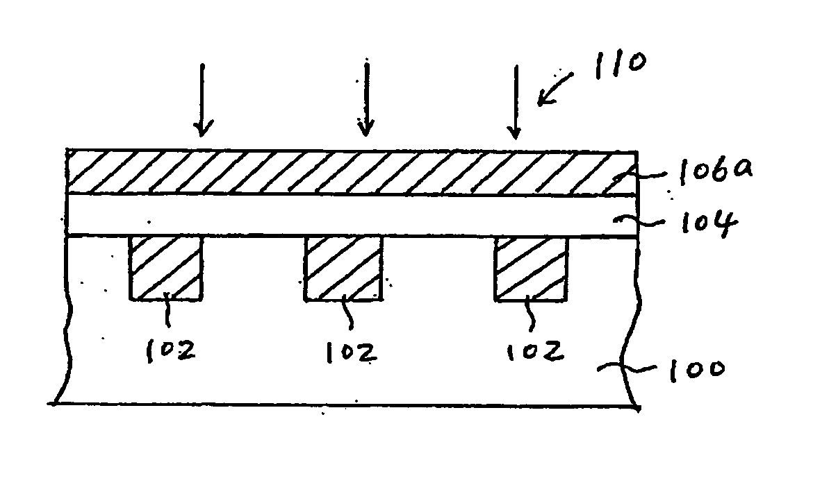
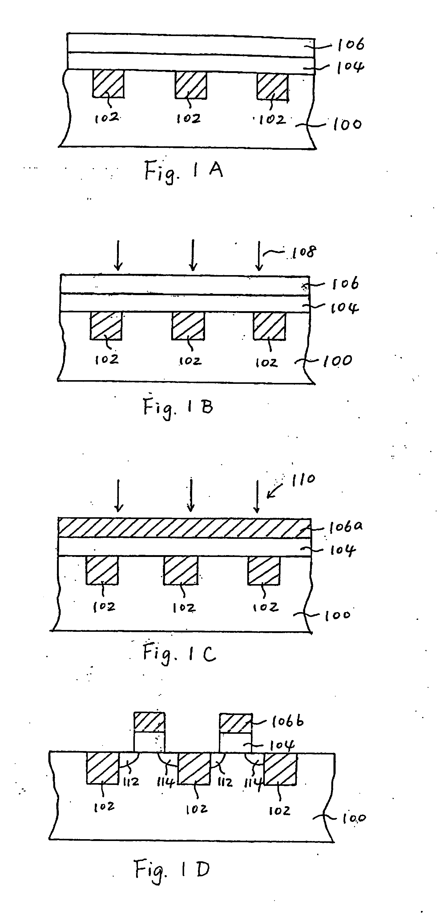
[0013]FIGS. 1A-1D are cross-sectional views of a structure formed with a method consistent with one embodiment of the present invention. Referring to FIG. 1A, the method of the present invention commences with providing a silicon substrate 100 and forming a plurality of isolation regions 102 between active areas (not shown) in substrate 100. Conventional techniques for insulating individual devices, such as local oxidation of silicon (LOCOS) and shallow trench isolation (STI), may be used to create isolation regions 102. Next, a gate oxide layer 104 is formed over substrate 100 and isolation regions 102 to a suitable thickness. Gate oxide layer 104 may be grown or deposited over substrate 100 with any conventional m...


PUM


Abstract

A method for manufacturing a semiconductor device includes providing a first layer, forming a plurality of isolation regions in the first layer, forming an insulating layer over the first layer, forming a second layer over the insulating layer, implanting one of helium, neon, krypton or xenon ions into the second layer, implanting boron ions into the second layer, patterning and etching the implanted second layer and the insulating layer, annealing at least the layer of implanted second layer to activate the implanted boron ions, and forming source and drain regions in the first layer.

Description

FIELD OF THE INVENTION [0001] The invention pertains in general to a method of manufacturing a semiconductor device, and more particularly, to a method of preventing undesired dopant diffusion in P-channel devices. BACKGROUND OF THE INVENTION [0002] A CMOS (complementary metal oxide semiconductor) device generally includes both a p-channel MOS transistor and an n-channel MOS transistor. Efforts have been made in the last decade to reduce the channel length of CMOS devices, one reason being a reduced channel length translates into a reduction in device size, and correspondingly a reduction in the cost of the semiconductor product into which the CMOS devices are incorporated. However, a reduced channel length often produces an unintended and undesirable leakage current in the channel region. This is known as “short-channel effect.” One of the causes of short-channel effect is the presence of unintended impurities in the channel regions. For p-channel MOS transistors, boron ions are of...

Claims


Application Information

Patent Timeline
IPC IPC(8): H01L21/265H01L21/28H01L21/8234H01L21/8238H01L29/78
CPCH01L21/265H01L21/26506H01L21/28026H01L29/78H01L21/823437H01L21/823828H01L21/28035H01L21/2658
Inventor WANG, TZU YU
Owner MACRONIX INT CO LTD
Why Eureka
Try Eureka