Method of fabricating a dual damascene interconnect structure

a technology of damascene and interconnect structure, which is applied in the manufacturing of semiconductor/solid-state devices, basic electric elements, electric devices, etc., can solve the problems of affecting performance, increasing the cost of integrated circuits and devices, and deteriorating the interconnect structur

Inactive Publication Date: 2005-03-17
APPLIED MATERIALS INC
View PDF5 Cites 26 Cited by
  • Summary
  • Abstract
  • Description
  • Claims
  • Application Information

AI Technical Summary

Problems solved by technology

These etch processes may form defects that degrade the interconnect structure.
Etch-related defects of the dual damascene interconnect structures may affect performance and increase costs of the integrated circuits and devices that include such structures.

Method used


Image

  • Method of fabricating a dual damascene interconnect structure
  • Method of fabricating a dual damascene interconnect structure
  • Method of fabricating a dual damascene interconnect structure

Examples


Embodiment Construction

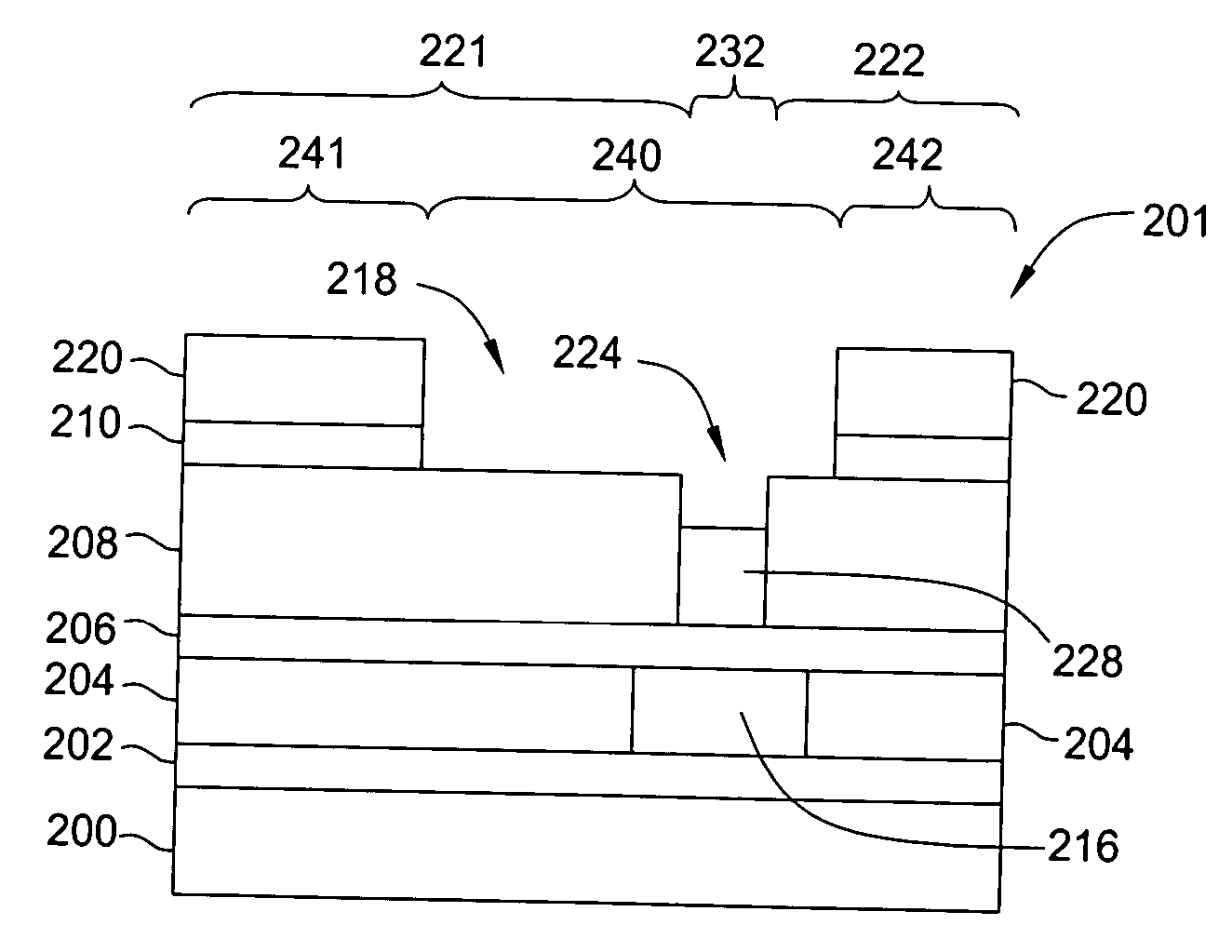
[0016] The present invention is a method of fabricating a dual damascene interconnect structure on a substrate (e.g., semiconductor substrate, such as a silicon (Si) wafer, and the like) using a very high frequency (VHF) plasma source. The method uses an etch process that in-situ forms a trench above a via hole of the structure and removes a barrier layer between the via hole and underlying conductive layer. In one embodiment, the etch process uses a very high frequency (VHF) high-density plasma and a selectively controlled substrate bias. Such a process can be performed in, for example, the ENABLER™ VHF etch chamber available from Applied Materials, Incorporated, located in Santa Clara, Calif.

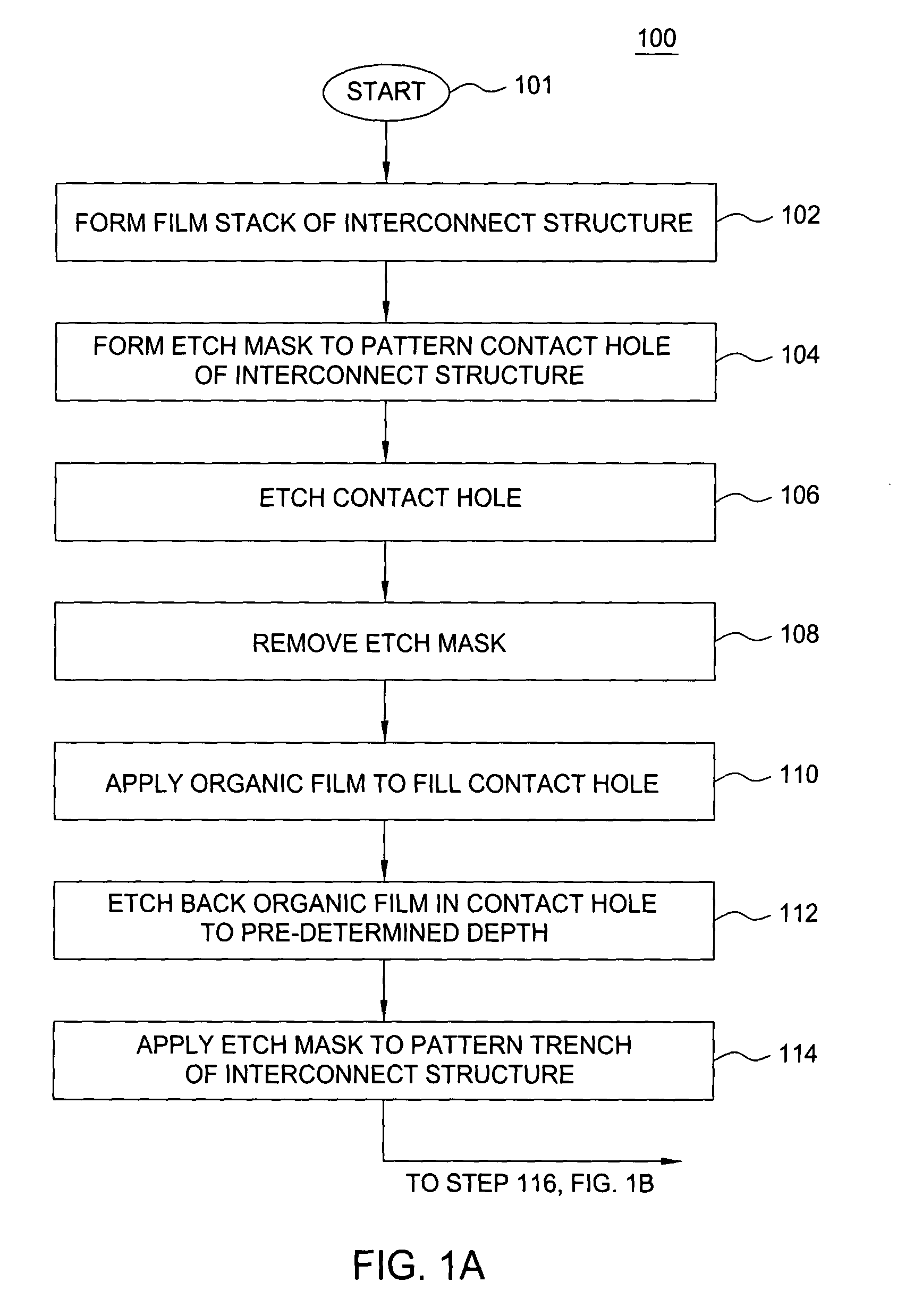
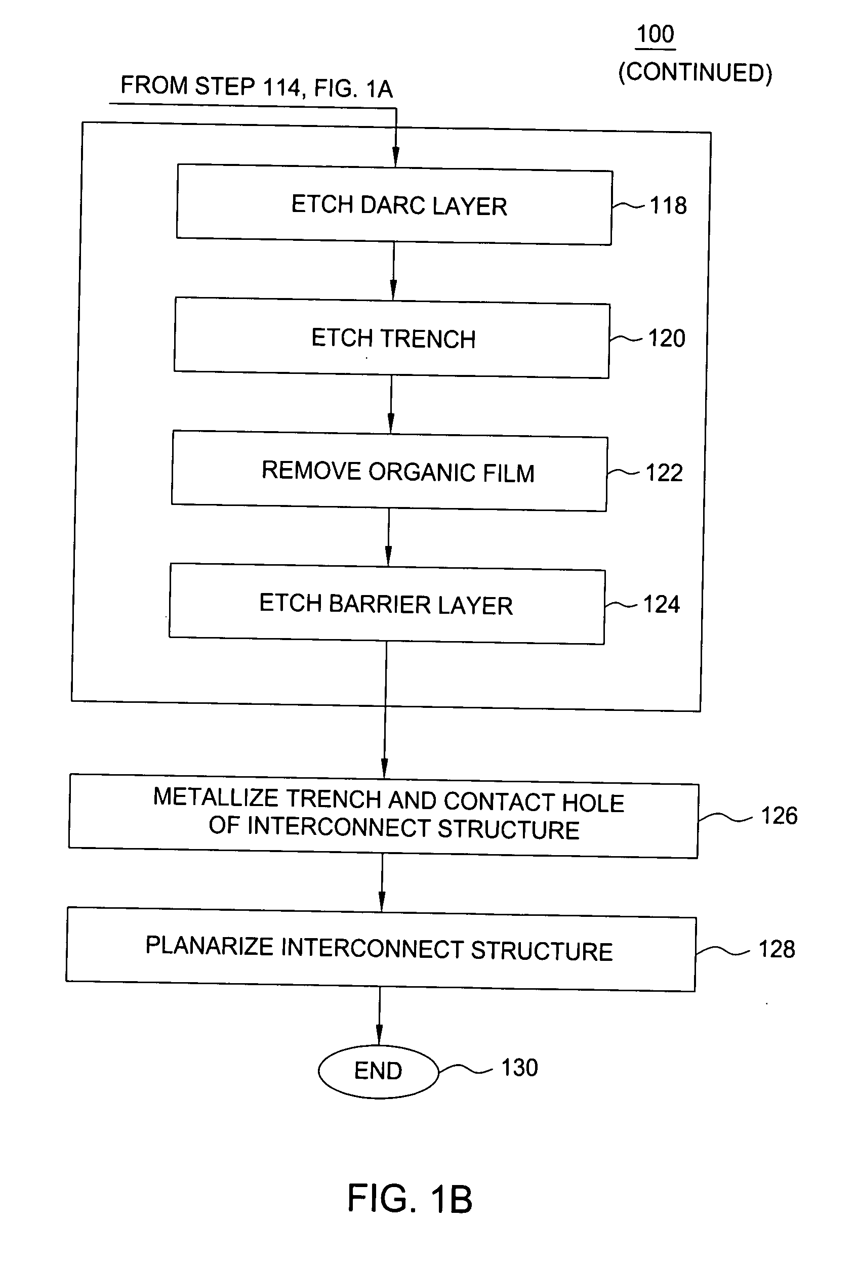
[0017]FIGS. 1A-1B depict a flow diagram of one embodiment of the inventive method for fabricating a dual damascene interconnect structure as a sequence 100. The sequence 100 comprises the processes that are performed upon a film stack of the dual damascene interconnect structure.

[0018]FIGS. ...


PUM


Abstract

A method of fabricating a dual damascene interconnect structure uses a very high frequency high-density plasma and selectively controlled substrate bias for in-situ etching a trench above a via hole of the interconnect structure and a barrier layer between the via hole and underlying conductive layer.

Description

BACKGROUND OF THE INVENTION [0001] 1. Field of the Invention [0002] The present invention generally relates to the fabrication of semiconductor integrated circuits. More specifically, the present invention relates to a method of fabricating interconnect structures in a semiconductor substrate processing system. [0003] 2. Description of the Related Art [0004] Integrated circuits (IC) are manufactured by forming discrete semiconductor devices on a surface of a semiconductor substrate, such as a silicon (Si) wafer. A multi-level network of interconnect structures is then formed to interconnect the devices. Copper (Cu) is the material of choice for interconnect structures of advanced IC devices having high circuit density. In addition to superior electrical conductivity, copper is more resistant than aluminum (Al) to electromigration, a phenomenon that may destroy a thin film conductive line during IC operation. [0005] In the semiconductor industry, much effort is spent in developing sm...

Claims


Application Information

Patent Timeline
Patent Type & Authority Applications(United States)
IPC IPC(8): H01L21/311H01L21/4763H01L21/768
CPCH01L21/02063H01L21/31116H01L21/76808H01L21/31144H01L21/31138
Inventor BERA, KALLOLDELGADINO, GERARDO A.ZHAO, ALLENYE, YAN
Owner APPLIED MATERIALS INC
Why Eureka
Try Eureka