
Ultra-high-frequency notch filter

a technology of ultra-high-frequency notch and filter, which is applied in the field of electromagnetic interference suppression, can solve the problems of affecting the intended performance of the filter, and reducing the efficiency of the filter, so as to reduce the number of parts used, reduce the cost of production, and reduce the effect of radiated emission

Inactive Publication Date: 2005-03-17
AVAYA INC
View PDF6 Cites 44 Cited by
  • Summary
  • Abstract
  • Description
  • Claims
  • Application Information

AI Technical Summary

Benefits of technology

This patent describes an apparatus and method for creating a notch filter for use in high-frequency applications. The apparatus includes a capacitor with a conductor that connects its terminals, which forms a parallel LC circuit with the capacitor. The notch filter can be easily constructed, tuned, and mounted on a printed circuit board. The technical effects of this invention include an effective notch filter that can be used at ultra-high frequencies, a compact size, and compatibility with surface-mount circuit-assembly techniques.

Problems solved by technology

The high-frequency transmission affected by such transmission lines make suppression of their radiated emissions a significant challenge, on account of the fact that radiated emissions, and the crosstalk to other signal lines caused thereby, increase as transmission frequency increases.
Although the use of notch filters to filter out EMI is known (see, e.g., U.S. Pat. No. 6,539,253), a technical challenge in developing a notch filter for EMI suppression is how to effectively deal with parasitic inductance and capacitance, which can deleteriously affect the intended performance of the filter.
At ultra-high transmission frequencies, even small parasitic effects can cause significant problems and therefore must be accounted for in the notch filter design.

Method used


Image

  • Ultra-high-frequency notch filter
  • Ultra-high-frequency notch filter
  • Ultra-high-frequency notch filter

Examples


Embodiment Construction

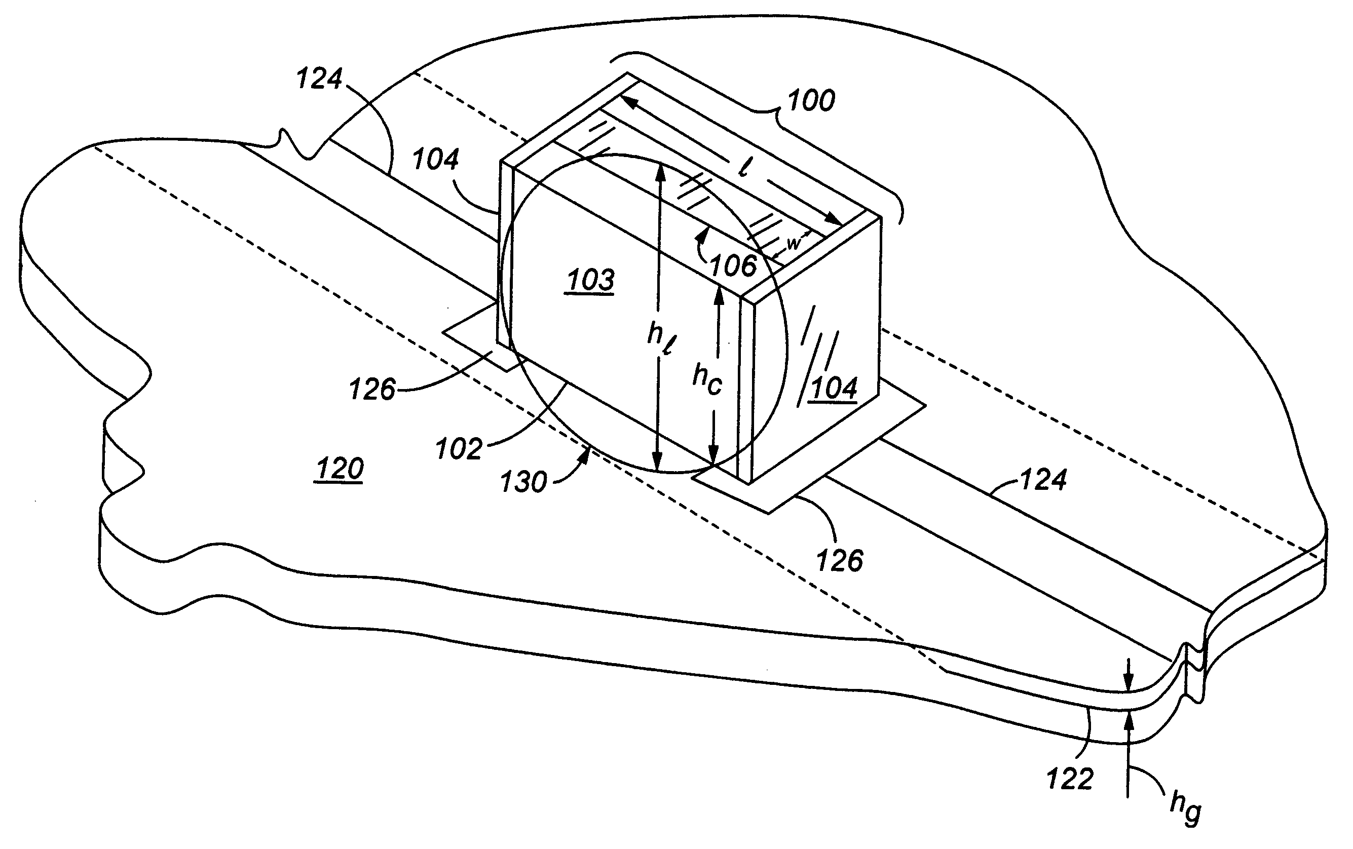
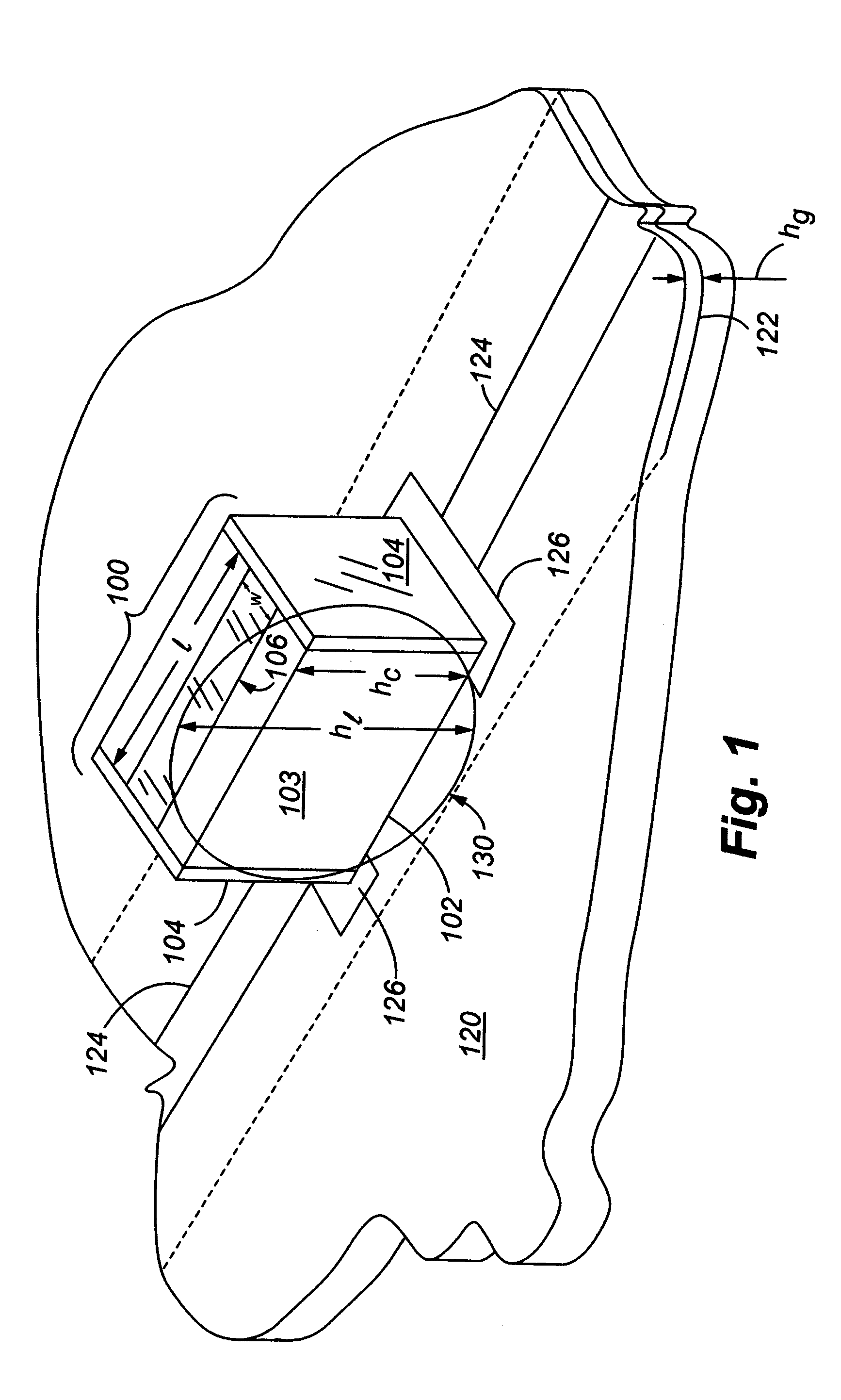
FIG. 1 shows an illustrative embodiment of a notch filter 100 mounted on a printed-circuit board (PCB) 120. Notch filter 100 spans two segments 124a and 124b of a printed-circuit conductor 124 carrying signals that are to be filtered for EMI. Each segment of conductor 124 terminates in a solder pad 126 to which notch filter 100 is electrically connected, e.g., by a component surface-mounting process.

Notch filter 100 consists of a capacitor 102, preferably a surface-mount capacitor, and a conductive trace 106 of width w and length l defined by (e.g., plated or printed on) and extending the length of body 103 of capacitor 102. Capacitor 102 is electrically connected to solder pads 126 by conductive terminals 104 that extend from opposite ends of body 103 of capacitor 102. Trace 106 is electrically connected to terminals 104, and acts as an inductor there between. Capacitor 102 and trace 106 together form a parallel inductive-capacitive (LC) circuit between the segments of conductor 1...


PUM


Abstract

An ultra-high-frequency notch filter (100) comprises a capacitor (102) defining a conductive trace (106) on its body (103) and extending between its terminals (104). The trace has an inductance that forms a parallel LC circuit with the capacitance of the capacitor. When mounted on a printed circuit board (120) to connect two segments of a signal line (124), the notch filter and a ground plane (122) of the PCB form a virtual conductive loop having an inductance and a capacitance whose product is the center frequency of the notch of the notch filter. The center ferquency is tuned by varying the width of the trace.

Description

TECHNICAL FIELD This invention relates to suppression of electromagnetic interference (EMI). BACKGROUND OF THE INVENTION Use of high-bandwidth transmission lines to implement local area networks (LANs) is becoming increasingly common. An example thereof is the Gigabit Ethernet LAN. The high-frequency transmission affected by such transmission lines make suppression of their radiated emissions a significant challenge, on account of the fact that radiated emissions, and the crosstalk to other signal lines caused thereby, increase as transmission frequency increases. A notch filter is designed to reject a band of frequencies while passing through all other frequencies. Although the use of notch filters to filter out EMI is known (see, e.g., U.S. Pat. No. 6,539,253), a technical challenge in developing a notch filter for EMI suppression is how to effectively deal with parasitic inductance and capacitance, which can deleteriously affect the intended performance of the filter. At ultra...

Claims


Application Information

Patent Timeline
Patent Type & Authority Applications(United States)
IPC IPC(8): H03H5/02H01P1/20H03H1/00H05K1/02
CPCH05K1/0233H05K2201/10636H05K2201/1006Y02P70/50H01P1/20
Inventor NORTE, DAVID A.YOON, WOONG K.
Owner AVAYA INC
Learn More