Transistor substrate, display device, and method of manufacturing transistor substrate and display device

a technology of transistor substrate and display device, which is applied in the direction of transistor, instruments, and tft, can solve the problems of unnecessarily increasing the size of tft, affecting the efficiency of the device, so as to facilitate further reduction of the device size, facilitate the effect of further reducing the size of the device, and high resistan

Inactive Publication Date: 2005-03-24
SANYO ELECTRIC CO LTD
View PDF11 Cites 19 Cited by
  • Summary
  • Abstract
  • Description
  • Claims
  • Application Information

AI Technical Summary

Benefits of technology

[0023] In addition, by selectively forming, for example, the channel length direction of the transistor in which a high resistance is required along a direction of the semiconductor layer with a low mobility, it is possible to form the transistor with a minimum area.
[0024] Because of this, a semiconductor device or display device with a high degree of integration can be obtained and it is possible to facilitate further reduction of the size of the device and further increase in the resolution.
[0025] Moreover, when a plurality of transistors are to be formed in one pixel in a display device, it is no longer necessary to employ significantly differing sizes for the transistors, allowing for effective usage of the pixel region and a higher resolution. In addition, because the transistors can be effectively placed, a display area within one pixel region can be increased, and, therefore, the aperture ratio can be improved.
[0026] By selectively forming a cap film above a channel region of a second transistor as in the present invention, it is possible to obtain different sizes for grain sizes of non-single crystalline silicon in the channel regions of the first and second transistors by merely simultaneously applying an annealing process to the semiconductor layers of the first and second transistors for crystallization.
[0027] By leaving the cap film in the completed transistor, it is possible to vary, between the first and second transistors, a thickness of an insulating film between the channel region and the gate electrode, and thus, it is possible to intentionally vary the current supply capability in the two transistors. Thus, even when a plurality of transistors having different current supply capability requirements are to be formed on the same substrate, it is not necessary to significantly vary the size of the transistors, which allows for effective usage of the space. Therefore, it is possible to further increase the degree of integration, reduce the size of the device, increase the resolution, and realize other beneficial effects.

Problems solved by technology

Because of this, the size of TFT is unnecessarily increased and the space is not efficiently used.
Moreover, a current driven light emitting element such as an EL element has a tendency to be degraded as current flows.
Therefore, it is not desirable to direct a current in an amount greater than the minimum required from the viewpoint of extending the lifetime of such a light emitting element.

Method used


Image

  • Transistor substrate, display device, and method of manufacturing transistor substrate and display device
  • Transistor substrate, display device, and method of manufacturing transistor substrate and display device
  • Transistor substrate, display device, and method of manufacturing transistor substrate and display device

Examples


first embodiment

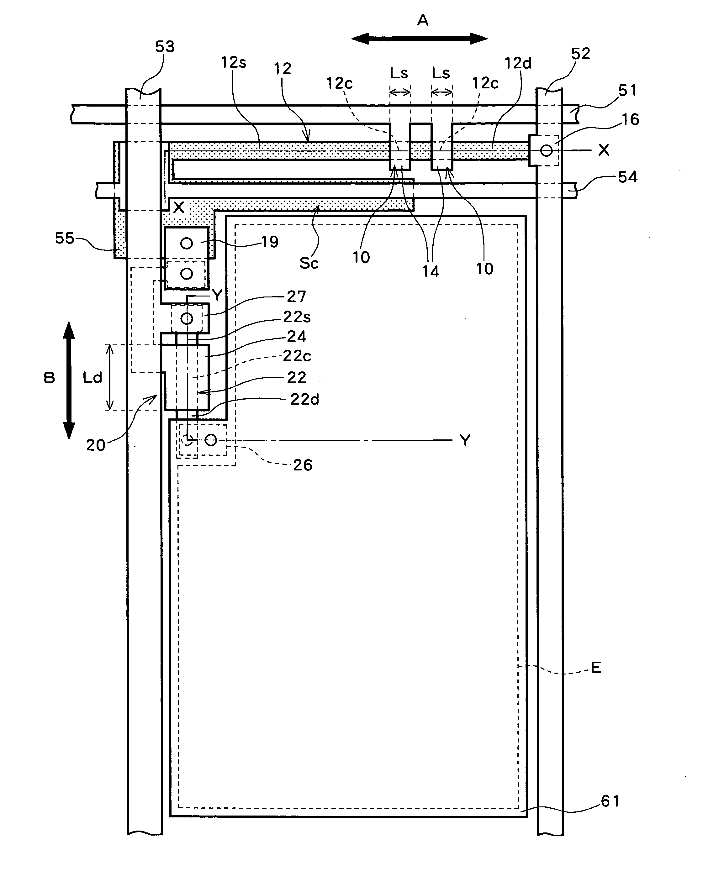
[0044]FIG. 4 is a diagram showing a pixel in an EL display device according to a first preferred embodiment of the present invention. A planar structure of a pixel in the EL display device will now be conceptually described referring to FIG. 4. The overall circuit structure of the EL display device is common to that shown in FIG. 1.

[0045] A plurality of gate signal lines 51 are placed along a horizontal direction and a plurality of drain (data) signal lines 52 and a plurality of power supply lines 53 are placed along a vertical direction. Two S-TFTs 10 connected in series with respect to a corresponding one of the drain signal lines 52, a storage capacitor electrode line 54, and a portion of a storage capacitor electrode 55 are placed between an emissive region E in which light emission of the EL element is viewed and the gate signal line 51.

[0046] Gate electrodes 14 of two S-TFTs 10 which are switching elements are connected to the gate signal line 51. More specifically, two gate...

second embodiment

[0069] An EL display device according to a second preferred embodiment of the present invention will now be described. FIG. 7 is a plan view showing a pixel of an EL display device according to the second preferred embodiment. Layers and structures identical to those shown on FIG. 4 are assigned the same reference numerals as those in FIG. 4 and will not be described again.

[0070] A portion of the gate signal line 51 is used as a gate electrode 14 and a channel region 12c is formed by forming a part of the semiconductor layer 12 in a “U” shape to form a region overlapping the gate electrode 14. This configuration also differs from that shown in FIG. 4 in that the channel length direction of the semiconductor layer 22 of the D-TFT 20 is different by 90° and is directed along a row direction which is an extension direction of the gate signal line 51. Thus, in the second embodiment, the conductive directions A′ and B′ which are channel length directions, that is, carrier moving directi...

third embodiment

[0071] An EL display device according to a third preferred embodiment of the present invention will now be described. FIG. 8 is a plan view showing a pixel in an EL display device according to the third preferred embodiment of the present invention. In this embodiment, a structure is employed in which two S-TFTs 10 and two D-TFTs 20 are provided in each pixel. With this configuration, it is possible to reduce manufacturing variation among D-TFTs 20 by placing a plurality of D-TFTs 20. This configuration is especially advantageous in structures having a wide manufacturing variation among TFTs, or in structures in which a demand for variation reduction is high.

[0072] The present invention is not limited to an EL display device and may be applied to other active matrix display devices in which a plurality of transistors are formed on the same substrate for driving and controlling a display element in each pixel. In addition, the present invention is not limited to a display device and...


PUM


Abstract

A device has a first transistor and a second transistor wherein a channel length direction of the first transistor extends along a first direction and a channel length direction of the second transistor extends along a second direction intersecting the first direction, and the second transistor is formed on a same substrate as the first transistor. A first channel region and a second channel region are formed in semiconductor layers which are simultaneously formed and a mobility of the semiconductor film has an anisotropy in the first and second directions. With this structure, transistors having different mobilities can be obtained while using the semiconductor films formed on the same substrate and from a same material. For example, it is possible to form a transistor in which a high resistance is required using a semiconductor layer of the same characteristics as that in a transistor in which a high speed operation is desired, on the same substrate and with a minimum area.

Description

CROSS-REFERENCE TO RELATED APPLICATIONS [0001] The priority Japanese Patent Applications, Numbers 2003-330123 and 2004-201925, upon which this patent application is based are hereby incorporated by reference. BACKGROUND OF THE INVENTION [0002] 1. Field of the Invention [0003] The present invention relates to a transistor substrate and a display device in which a plurality of transistors are used, and methods of manufacturing the transistor substrate and the display device. [0004] 2. Description of the Related Art [0005] Recently, electroluminescence (hereinafter simply referred to as “EL”) display devices in which an EL element is used have attracted much attention as new display devices. In particular, active matrix EL display devices having, in each pixel, a switching thin film transistor (S-TFT) for selecting a pixel and a driving thin film transistor (D-TFT) for supplying power for driving the EL element based on an output of the switching transistor have drawn interest for thei...

Claims


Application Information

Patent Timeline
Patent Type & Authority Applications(United States)
IPC IPC(8): H01L51/50G09F9/30H01L21/20H01L21/336H01L21/77H01L21/84H01L27/12H01L27/32H01L29/786
CPCH01L27/1285H01L29/78675H01L29/78645H01L27/1296H01L27/1281
Inventor NISHIKAWA, RYUJIIMAO, KAZUHIROWAKITA, KENYONEDA, KIYOSHI
Owner SANYO ELECTRIC CO LTD
Why Eureka
Try Eureka