Position measurement mehtod, exposure method, exposure device, and manufacturing method of device

Inactive Publication Date: 2005-03-24
NIKON CORP
View PDF1 Cites 12 Cited by
  • Summary
  • Abstract
  • Description
  • Claims
  • Application Information

AI Technical Summary

Benefits of technology

[0027] According to this method of manufacturing a device, the accuracy of exposure to

Problems solved by technology

In such a case, there is a possibility that measurement error will occur

Method used


Image

  • Position measurement mehtod, exposure method, exposure device, and manufacturing method of device
  • Position measurement mehtod, exposure method, exposure device, and manufacturing method of device
  • Position measurement mehtod, exposure method, exposure device, and manufacturing method of device

Examples


Embodiment Construction

[0045] In the following, various preferred embodiments of the present invention will be explained with reference to the figures.

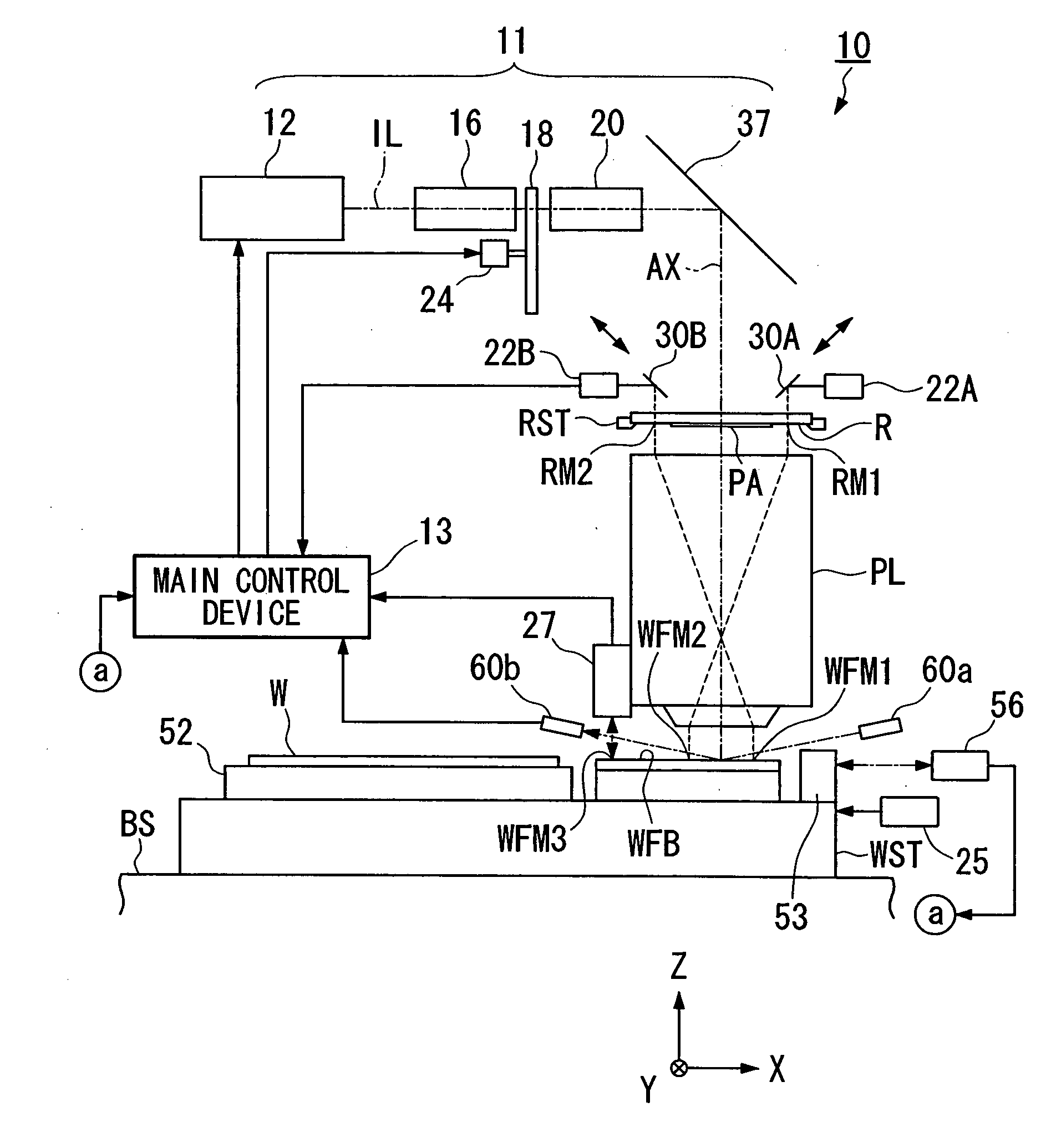
[0046]FIG. 1 is a figure showing the schematic form the structure of a reduction projection type exposure device which is used for manufacture of a semiconductor device. This projection exposure device 10 is a scanning type exposure device of the step-and-scan type, which transcribes a circuit pattern which has been formed upon a reticle R (which acts as a mask) into each shot region upon a wafer W (which acts as a substrate) while synchronously shifting the reticle R and the wafer W in a one dimensional direction.

[0047] This projection exposure device 10 comprises an illumination system 11 which includes a light source 12, a reticle stage RST which holds the reticle R, a projection optical system PLwhich projects an image of the pattern which is formed upon the reticle R onto the wafer W, a wafer stage WST which acts as a substrate stage for supporting t...


PUM


Abstract

With this position measurement method, a mark which has been formed upon an object is illuminated with an illumination beam, a beam which is generated from this mark is picked up via an observation system, and the resultant image signal is signal processed so as to measure positional information which is related to the mark. This signal processing is performed based upon information related to the noise which is included in the component dependent upon the amount of light which is included in the image signal, and upon said image signal. As a result, it is possible to measure the positional information for the mark with good accuracy, even if noise is included in the image signal.

Description

BACKGROUND OF THE INVENTION [0001] 1. Field of the Invention [0002] The present invention relates to a position measurement method for measuring positional information related to the position of a mark by picking up an image via an observation system of a mark which is formed upon an object, and by performing signal processing upon this image signal; and in particular relates to a technique which is utilized in a exposure method and a exposure device which are used in a manufacturing process for a device such as a semiconductor element or a liquid crystal display element or the like. This application is a continuation application based on PCT / JP2003 / 06941 designating U.S.A. filed on Jun. 2, 2003. [0003] 2. Description of the Related Art [0004] While performing a manufacturing process for an electronic device such as a liquid crystal display element or the like, a plurality of layers of a circuit pattern are formed over one another in a predetermined positional relationship upon a su...

Claims


Application Information

Patent Timeline
IPC IPC(8): G03F9/00
CPCG03F9/7092G03F9/7076
Inventor KOBAYASHI, MITSURU
Owner NIKON CORP
Why Eureka
Try Eureka