Mask blank, method for manufacturing transfer mask, and method for manufacturing semiconductor device

Active Publication Date: 2017-06-15
HOYA CORP
View PDF6 Cites 12 Cited by
  • Summary
  • Abstract
  • Description
  • Claims
  • Application Information

AI Technical Summary

Benefits of technology

[0057]According to the mask blank of this invention, such fine transfer pattern as the SRAF pattern can be formed with high accuracy. In other words, according to the mask blank of this invention, the etching rate is the lowest for the upper layer of the light shielding film, and hence the pattern of the upper layer is less susceptible to the side etching. As a result, the light shielding film pattern to which the shape of the transfer pattern, which is formed in the resist film or the hard mask film, is transferred substantially accurately can be formed, and hence the accuracy of the pattern, which is to be formed in the light-semitransmissive film using the light shielding film pattern as the mask, can be increased. Moreover, the etching rate of the lower layer of the light shielding film is the next lowest to that for the upper layer, and

Problems solved by technology

Therefore, the dimensional accuracy of a pattern formed on the transfer mask di

Method used


Image

  • Mask blank, method for manufacturing transfer mask, and method for manufacturing semiconductor device
  • Mask blank, method for manufacturing transfer mask, and method for manufacturing semiconductor device
  • Mask blank, method for manufacturing transfer mask, and method for manufacturing semiconductor device

Examples


Example

EXAMPLE

[0126]Now, the present invention is described in more detail by way of Examples.

Example

Example 1

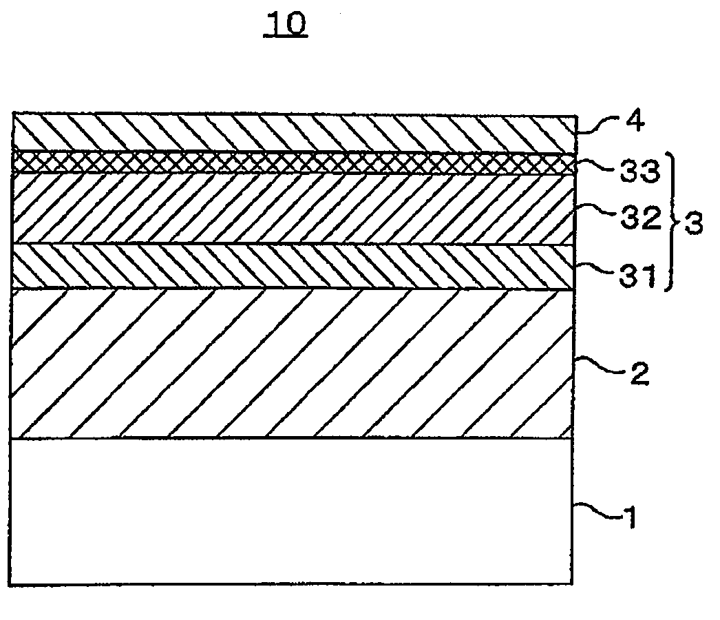
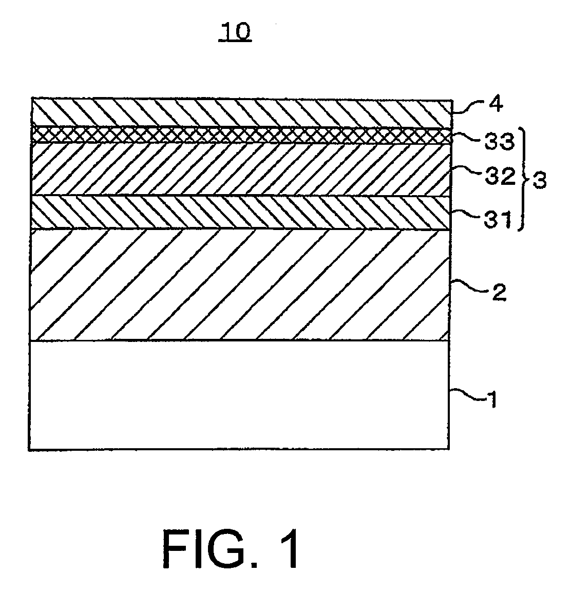
[0127]Example according to this invention relates to a mask blank for use in manufacturing of a halftone-type phase shift mask using the ArF excimer laser having the wavelength of 193 nm as the exposure light.

[0128]The mask blank used in this Example has the structure in which the light-semitransmissive film 2, the light shielding film 3 having the three-layer laminated structure, and the hard mask film 4 are laminated in the stated order on the transparent substrate (glass substrate) 1 as illustrated in FIG. 1. This mask blank was manufactured as follows.

[0129]As the glass substrate, a synthetic quartz substrate (having a size of about 152 mm by about 152 mm and a thickness of 6.35 mm) was prepared.

[0130]Then, the above-mentioned synthetic quartz substrate was placed in a sheet-type DC sputtering apparatus, and a MoSiN light-semitransmissive film (phase shift film) made of molybdenum, silicon, and nitrogen was formed to have a thickness of 69 nm on the synthetic quartz sub...

Example

[0151]The mask blank in this Comparative Example was used to manufacture a halftone-type phase shift mask in a method similar to that in Example 1.

[0152][Evaluation of Light Shielding Film Pattern]

[0153]When a cross-sectional shape of the light shielding film pattern was checked after the above-mentioned step of patterning the light shielding film 3 (step in FIG. 2C) was ended, the cross-sectional shape as illustrated in FIG. 4 was observed. More specifically, the light shielding film had a shape that was deeply hollowed by the erosion due to the etching in the wall surface of the pattern. Moreover, line widths were thinner than those in the pattern of the hard mask film, and had a tendency toward a large divergence in dimension from the hard mask film pattern.

[0154]Moreover, as in Example, cleaning was performed after the step of patterning the light shielding film 3 (step in FIG. 2C) was ended, and when a state of the pattern of the lines and spaces of 40 nm (corresponding to a pa...


PUM


Abstract

In order to form a fine mask pattern with high accuracy, in a mask blank in which a light-semitransmissive film, a light shielding film, and a hard mask film are laminated in the stated order on a transparent substrate, the light-semitransmissive film containing silicon and additionally nitrogen, the hard mask film containing silicon or tantalum, and additionally oxygen, the light shielding film having the laminate structure of a lower layer, an intermediate layer, and an upper layer and containing chromium, conditions on the light shielding film are adjusted so that etching rates using a mixture gas of chlorine and oxygen are the lowest for the upper layer and the next lowest for the lower layer.

Description

TECHNICAL FIELD[0001]This invention relates to a method of manufacturing a transfer mask used in manufacturing a semiconductor device, and a mask blank used in manufacturing the transfer mask.BACKGROUND ART[0002]In general, in a manufacturing step of a semiconductor device, a fine pattern is formed using a photolithography method. Further, in forming the fine pattern, a large number of transfer masks (also generally called photomasks) are generally used. In a transfer mask, in general, a light shielding blocking fine pattern formed of a metal thin film or the like is provided on a transparent glass substrate. The photolithography method is also used in manufacturing this transfer mask.[0003]The transfer mask is an original plate for transferring the same fine pattern in high volume. Therefore, the dimensional accuracy of a pattern formed on the transfer mask directly affects the dimensional accuracy of the fine pattern to be manufactured. As the degree of integration of a semiconduc...

Claims


Application Information

Patent Timeline
IPC IPC(8): G03F1/32H01L21/306H01L21/308
CPCG03F1/32H01L21/30604H01L21/3086H01L21/3081G03F1/48G03F1/80G03F1/20
Inventor SHISHIDO, HIROAKINOZAWA, OSAMU
Owner HOYA CORP
Why Eureka
Try Eureka