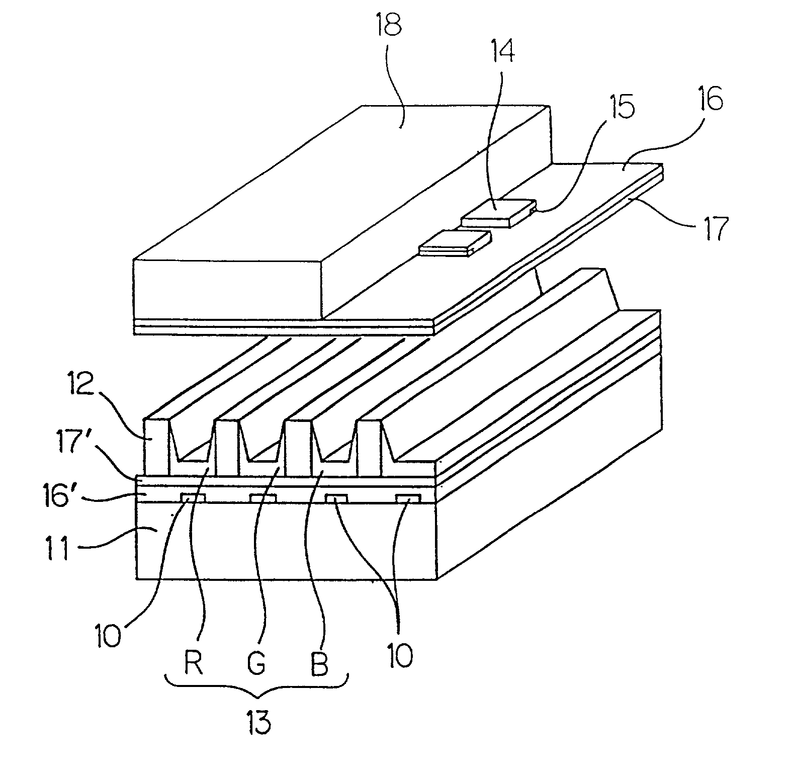
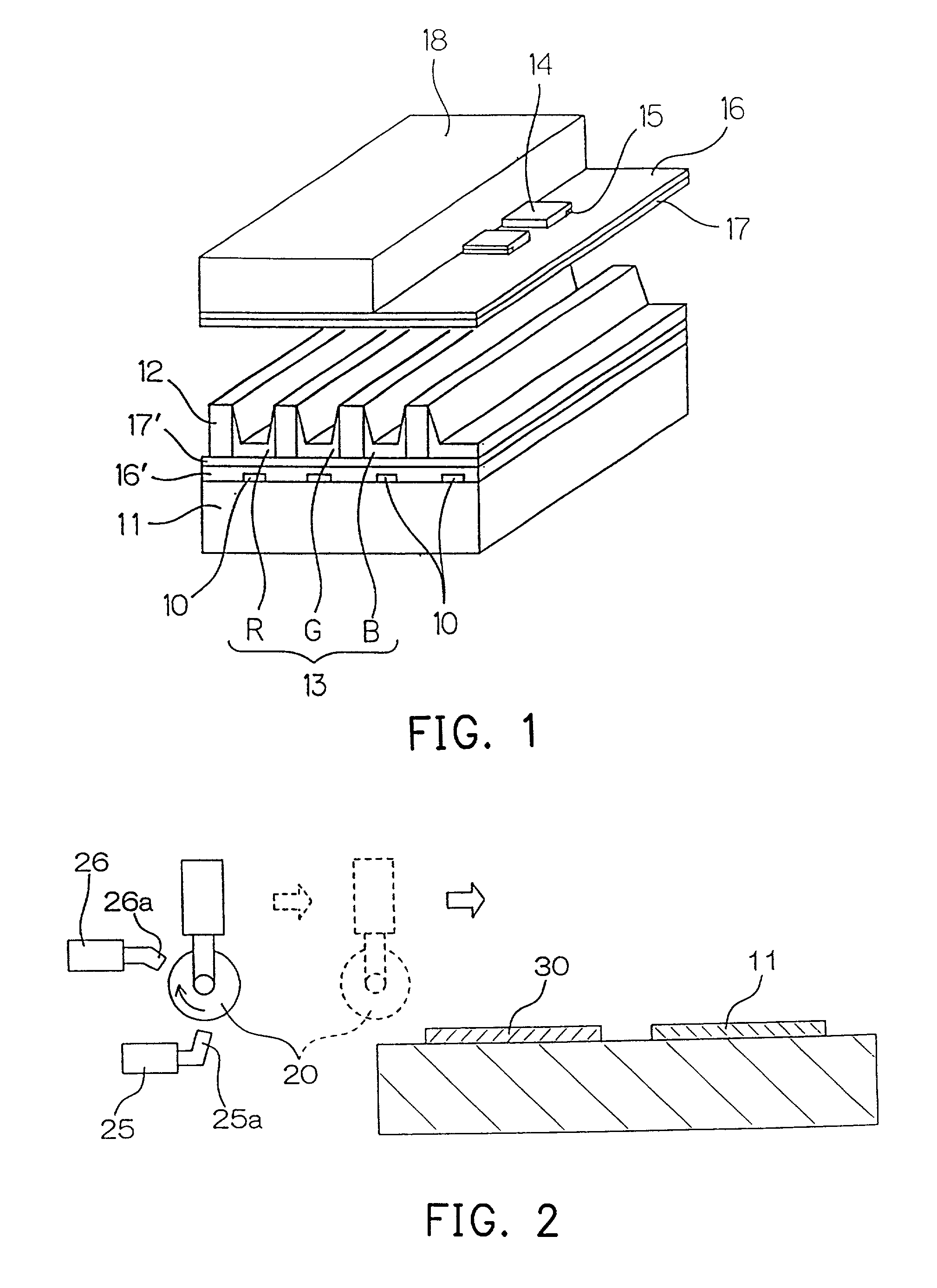
However, there are certain limitations on
miniaturization and rarefaction due to their structures.
However, the manufacturing cost for a PDP is very high at present, which is a barrier to commercialize the home-oriented
display device.
The amount of the removed
silver paste in the developing process would be too much and would not be economical.
However, there are no effective methods for solving the cost issues in the recycle and reuse processes.
Therefore, it becomes more obvious that the paste utility rate is low and the manufacturing cost increases.
Therefore, the manufacturing of electrode by
photolithography is very disadvantageous in the aspect of cost.
Conventionally, the printing method is not suitable for forming a very tiny and highly precise pattern for the PDP electrode.
In addition, among the various printing methods, even though the intaglio
offset printing method that is the most superior in printing accuracy is used, it still has a drawback (pinhole) that the printing shape deteriorates due to the repeated printing.
Also, from the point of view of productivity, it is very difficult to use the printing method for making the electrode substrate for a PDP panel.
In addition, because the pattern is made by the printing method, it is very low in price in comparison with that of the conventional PDP substrate.
Therefore, there are problems that the operational time stops and the productivity reduces drastically.
However, the ink
solvent cannot be sufficiently removed only by contacting with the absorber.
In contrast, there is a problem that dust from the absorber may adhere on the surface of the printing blanket.
However, any one of the methods disclosed above requires the complicated apparatus (blanket body and roller member) and the removing effect of the ink solvent is not adequate.
As the
display device becomes larger and larger, the
exposure device and developing
etching device in a photolithographic process must become large as well, thereby the enlargement of the related devices is very disadvantageous in the consideration of cost.
In addition, because the running cost of the devices is very high, it is very difficult to reduce the required cost to half of that of the current PDP manufacturing process.
There are many printing methods, of which a
screen printing cannot truly reproduce the patterns with a
line width less than 100 .mu.m.
There are also problems that broken lines always occurring.
Therefore, the
screen printing cannot satisfy the printing accuracy (surface accuracy .+-.10 .mu.m) required by the electrode.
However, there is a problem that the
layer thickness obtained by a planographic
offset printing, one of the offset printing methods, cannot be over 0.5 .mu.m each time.
Considering that the thickness of the conductive pattern formed by printing has to be several .mu.m, the planographic offset printing must be repeatedly performed from several times to ten times. As a result, the productivity and the printing accuracy reduce significantly.
The manufacturing cost also increases.
As a result, due to the repeated printing, there are problems that the productivity and the printing accuracy reduce, leading to an increase of the manufacturing cost.
In addition, because the thickness of the ink layer obtained by a relief offset printing each time is also thin, the same problems as described above are resulted.
Because of the ink
effusion, also known as marginal zone, generated around the pattern in the
relief printing, it is very difficult to truly reproduce the pattern.
The ink residues contaminate the non-pattern portion and reduce the printing accuracy.
Non-alkali glass, however, is very expensive.
There are some problems in offset printing.
As a result, the thickness and the
line width are uneven, causing problems like a broken pattern or a deteriorated printed shape.
In addition, pinhole problem also occurs.
When the surface temperature T.sub.B of the printing blanket is heated to a temperature lower than 40.degree. C., the
vaporization and the removal of the solvent that permeats into the surface printing layer is very ineffective.
On the other hand, when the surface temperature T.sub.B of the printing blanket is heated to a temperature higher than 200.degree. C., it causes thermal degradation and deterioration of the rubber that forms the surface printing layer.
When the surface temperature T.sub.B of the printing blanket keeps a rising status because of the foregoing heating process, the
thermal expansion of the intaglio occurs as the blanket and the intaglio are in contact in the printing process, which causes a problem that the printing accuracy reduces.
If the printing process is performed (when the printing blanket is in contact with the intaglio) in a state that the surface temperature T.sub.B of the printing blanket with respect to the surface temperature T.sub.P of the intaglio exceeds 5.degree. C., the printing accuracy is adversely affected when the variation of surface temperature T.sub.P exceeds 1.degree. C.
If the surface temperature T.sub.B with respect to the surface temperature T.sub.P is lower than -5.degree. C., the printing accuracy is adversely affected when the surface temperature T.sub.P exceeds 1.degree. C. as intaglio is in contact with the print blanket.
When the foregoing volume increasing rate is over 20%, the wettability variation of the surface of the printing blanket becomes large, and therefore the printing process cannot be stably performed.
As will be described in greater detail below, problem, such as the
line width of the pattern is being widened, may occur.
In such a case, because the variation of the
surface layer is too large when the conductive ink is transcribed from the printing blanket to the rear substrate, it is impossible toprecisely print the pattern because of the foregoing reasons.
Namely, the surface wittability increases such that the line width of the printed pattern is widened, and therefore the tiny
dirt on the intaglio surface is transcribed, which causes a problem of a reduction of the transferability of the ink to the rear substrate.
If the
hardness of the
surface layer exceeds the above range (the printing blanket is too hard), the
surface layer cannot be sufficiently pressed into the cavities of the intaglio even though the printing blanket is pressed to be in contact with the intaglio.
As a result, the conductive ink that is filled in the cavities cannot be sufficiently transcribed, failing to perform the high-precise printing.
In contrast, if the
hardness of the surface layer is lower than the above range (the printing blanket is too soft), the deformation of the surface layer is too large when the printing blanket is pressed to be in contact with the intaglio or the glass substrate, failing to perform the high-precise printing.
However, if the thickness is over 1.5 mm, the deformation of the rubber becomes large.
If the thickness of the surface layer is lower than 1 .mu.m, pinholes occur and the printing accuracy reduces.
If the amount of the
metal powder that is added is less than the above range, the resistance of the
metal pattern cannot be reduced.
In contrast, if the amount of the
metal powder that is being added is larger than the above range, the combining force of the resin binder that combines the metal powders is weak.
Therefore the printability of the conductive ink reduces, which degrades the printing shape and reduces the transferability of the conductive ink from the printing blanket to the glass substrate.
In contrast, if the amount of the resin binder that is added is larger than the above above, the resistance of the baked pattern cannot be reduced.
If the
boiling point of the solvent is lower than 150.degree. C., it is not easy to dry the glass substrate during the printing process and the printing property unavoidably changes.
Additionally, it is potentially that the composition of the conductive ink easily changes with time.
If the
viscosity of the conductive ink composition is lower or higher than the above range, the printing suitability thus reduces, which the tiny pattern may not be formed.
If the line width is lower than the above range, the line is easily broken and the
conductivity of the electrode pattern may get worse.
On the contrary, if the line width is higher than the above range, the electrode pattern may not be suitable for the tiny pixel pattern of the PDP.
When the thickness of the pattern is below the above range, the line is easily broken and the
conductivity of the electrode pattern may get worse.
On the contrary, if the thickness of the pattern is higher than the above range, the
electrode material wastes and therefore the material cost increase, which causes a problem reducing the
surface smoothness of the electrode pattern.
Because the solvent used in comparison example 1 causes the printing blanket to swell to a large extemt, if the printing process is repeatedly performed, the printing quality apparently reduces, especially in the increment of the pattern line width.
As a result, the accuracy of the pattern required by the PDP panel is not sufficient and the printing durability of the printing blanket is also insufficient.
However, the printing accuracy is very low and cannot be kept within a range of .+-.50 .mu.m on the 42-inch panel surface.
Therefore, the accuracy is insufficient for practice.

