Thin film capacitor and electronic circuit component

a technology of electronic circuit components and thin film capacitors, which is applied in the incorporation of printed capacitors, transistors, printed electric components, etc., can solve the problems of reducing the dielectric breakdown voltage and the likely event of shorting between the electrodes, so as to prevent the reduction of dielectric strength or shorting, improve the yield of capacitors, and enhance the accuracy of capacitors

Inactive Publication Date: 2007-11-13
HITACHI LTD
View PDF30 Cites 10 Cited by
  • Summary
  • Abstract
  • Description
  • Claims
  • Application Information

AI Technical Summary

Benefits of technology

[0029]The area relationship between the lower electrode, dielectric layer, the opening portion of the insulator on the lower electrode and the upper electrode is preferably; dielectric layer≧lower electrode≧opening portion of insulators≧upper electrode. In order to prevent reduction of dielectric strength or shorting between the electrodes, it is preferable to form a dielectric layer at the side face of the lower electrode and further, the area of the dielectric layer is preferably larger than that of the lower electrode. Since the lower electrode end portion is covered by the insulator, the area of the opening portion of the insulator on the lower electrode is smaller than that of the lower electrode. Further, since the patterning accuracy of the upper electrode is better than the opening accuracy of the insulator, it is preferable to form the area of the upper electrode to be smaller than that of the opening of the insulator on the lower electrode. Namely, when the area of the upper electrode is formed smaller than that of the insulator of the opening on the lower electrode, the capacitance of the capacitor is determined by the area of the upper electrode, therefore, the accuracy of the capacitor is enhanced and the yield thereof can be improved.

Problems solved by technology

Still further, when the thickness of the lower electrode exceeds more than six times the thickness of the dielectric layer, problems such as reduction of the dielectric breakdown voltage and shorting between the electrodes are likely to occurs.

Method used


Image

  • Thin film capacitor and electronic circuit component
  • Thin film capacitor and electronic circuit component
  • Thin film capacitor and electronic circuit component

Examples


embodiment 1

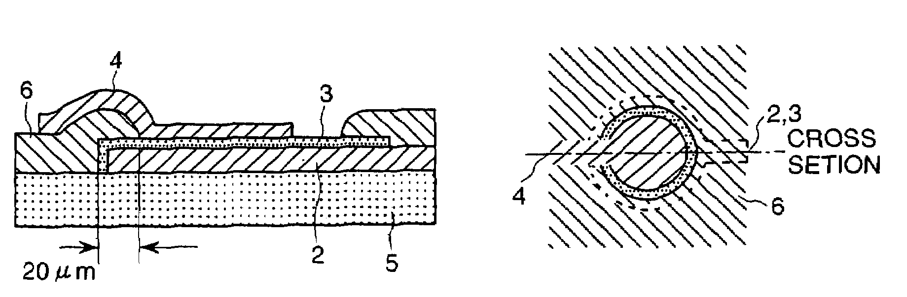
[0041]FIG. 3-1 is a cross sectional view of a thin film capacitor representing an embodiment of the present invention. FIG. 3-2-a is a plan view of the thin film capacitor of the present embodiment. FIG. 3-2-b is an exploded view of the thin film capacitor of the present embodiment. Further, FIG. 3-1 is the cross sectional view taken along the cross sectional plan indicated in FIG. 3-2-a.

[0042]The thin film capacitor was produced in the following manner.

[0043]Platinum film of 2 μm was formed on a glass substrate 5 by sputtering method. Subsequently, positive type liquid resist OFPR800, 500 cp(product of Tokyo Ohka) is coated and after performing drying, exposing and developing process, a resist mask for a lower electrode was formed. Then, dry etching was performed by ion milling to remove unnecessary platinum portions and after removing the resist mask the lower electrode 2 was formed. In the present embodiment, the shape of the lower electrode is formed in a circle as shown in FIG...

embodiment 2

[0048]In the like manner as in embodiment 1 thin film capacitors were produced. In this instance, benzocyclo butene resin cycloten 4026(product of Dow Chemical) was spin coated to form the insulator and after prebaking the same through the exposing and developing process, like embodiment 1 the opening end portion of the benzocyclo butene resin was formed to locate at the inner side of the lower electrode end portion by 20 μm. The resin was hardened at 250° C. / 1 hour under nitrogen atmosphere and an insulator of 10 μm was formed.

[0049]A current feed check was performed for 20 pieces of the thin film capacitors produced according to the above method. The result thereof is shown in FIG. 10. Although the defective rate of comparison thin film capacitors was 14 / 20, the defective rate of the present embodiment was 0 / 20.

embodiment 3

[0050]Thin film capacitors were produced in a like manner as in embodiment 1. In this instance, the thin film capacitors were produced by making use of a material having low dielectric loss tangent, which was prepared in the following method as the insulator.

[0051]Three raw materials of synthesized 1,2-bis(vinylphenyl)ethane of 30 weight parts, cyclic polyolefin Zeonex 480(product of Nihon Zeon) of 70 weight parts and hardening catalyst perhexyne 25B of 0.3 weight parts were resolved in xylene solvent so that solid component assumes 38% to produce a varnish.

[0052]The varnish was spin coated and the varnish was step cured on a hot plate in 120° C. / 2 minutes and then 200° C. / 5 minutes to form an insulator of 10 μm. On the cured varnish positive type liquid resist OFPR 800,500 cp was spin coated and after drying the same, through exposing and developing process a resist mask was formed in such a manner that the opening end portion thereof locates at the inner side of the lower electrod...


PUM

PropertyMeasurementUnit
thicknessaaaaaaaaaa
thicknessaaaaaaaaaa
thicknessaaaaaaaaaa

Abstract

A thin film capacitor comprising a lower electrode formed on a predetermined surface, a dielectric layer formed on the lower electrode, and an upper electrode formed on the dielectric layer, wherein the end portion of the lower electrode is further covered by an insulator other than the dielectric layer.

Description

FIELD OF THE INVENTION[0001]The present invention relates to a thin film capacitor and an electronic circuit component.BACKGROUND ART[0002]A schematic cross sectional view of a conventional thin film capacitor is shown in FIG. 1. After forming a metal film on a formed substrate 1 such as by a sputtering device, a resist is formed through a conventional photolithograph process and a lower electrode 2 is formed such as by dry etching. Thereafter, a dielectric material is formed by sputtering or CVD, then a dielectric layer 3 is formed through photolithography. Further, an upper electrode 4 is formed in the same manner as in the formation of the lower electrode. Through the above processes a conventional thin film capacitor was manufactured. Further, JP-A-9-289611 discloses a thin film capacitor in which, after forming a sidewall face inclined at a gentle angle at the edge portion of a lower electrode as shown in FIG. 2, a dielectric layer 3 and an upper electrode 4 are formed. As the ...

Claims


Application Information

Patent Timeline
Patent Type & Authority Patents(United States)
IPC IPC(8): H01L29/00H01L23/498H01L23/64H01L27/08H05K1/16
CPCH01L27/0805H01L23/49822H01L2924/15311H05K1/162H01L2924/0002H01L2924/00
Inventor OGINO, MASAHIKOSATOH, TOSHIYAMIWA, TAKAONABATAME, TOSHIHIDEAMOU, SATORU
Owner HITACHI LTD
Why Eureka
Try Eureka