Method and apparatus for wafer mechanical stress monitoring and wafer thermal stress monitoring

a mechanical stress monitoring and thermal stress monitoring technology, applied in mechanical measuring arrangements, lapping machines, instruments, etc., can solve the problems of affecting the surface quality of wafers, excessive dishing and erosion, and affecting the process quality of polishing interfaces, etc., to achieve the effect of relieving the stress condition

Inactive Publication Date: 2005-03-31
LAM RES CORP
View PDF28 Cites 26 Cited by
  • Summary
  • Abstract
  • Description
  • Claims
  • Application Information

AI Technical Summary

Benefits of technology

[0010] In accordance with still yet another embodiment, a process development tool configured to monitor stress conditions experienced by a substrate during semiconductor processing operations is provided. The process tool includes a sensor configured to monitor a signal indicative of a stress experienced by a substrate during processing operations within the process development tool. A computing device is in communication with the sensor. The computing device is configured to create a stress map from the signal. The computing device is further configured to analyze the stress map to identify any stressed regions of the substrate so that the computin

Problems solved by technology

Since the chemical etching is exponentially sensitive to the thermal conditions, a single hot spot on the surface of the wafer may adversely impact the wafer surface quality.
Moreover, with respect to low-k dielectrics app

Method used


Image

  • Method and apparatus for wafer mechanical stress monitoring and wafer thermal stress monitoring
  • Method and apparatus for wafer mechanical stress monitoring and wafer thermal stress monitoring
  • Method and apparatus for wafer mechanical stress monitoring and wafer thermal stress monitoring

Examples


Embodiment Construction

[0027] Several exemplary embodiments of the invention will now be described in detail with reference to the accompanying drawings. In the following description, numerous specific details are set forth in order to provide a thorough understanding of the present invention. It will be understood, however, to one skilled in the art, that the present invention may be practiced without some or all of these specific details. In other instances, well known process operations have not been described in detail in order not to unnecessarily obscure the present invention.

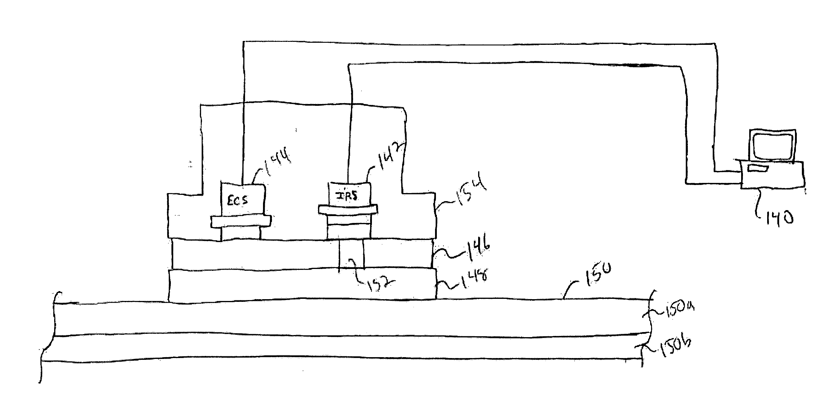
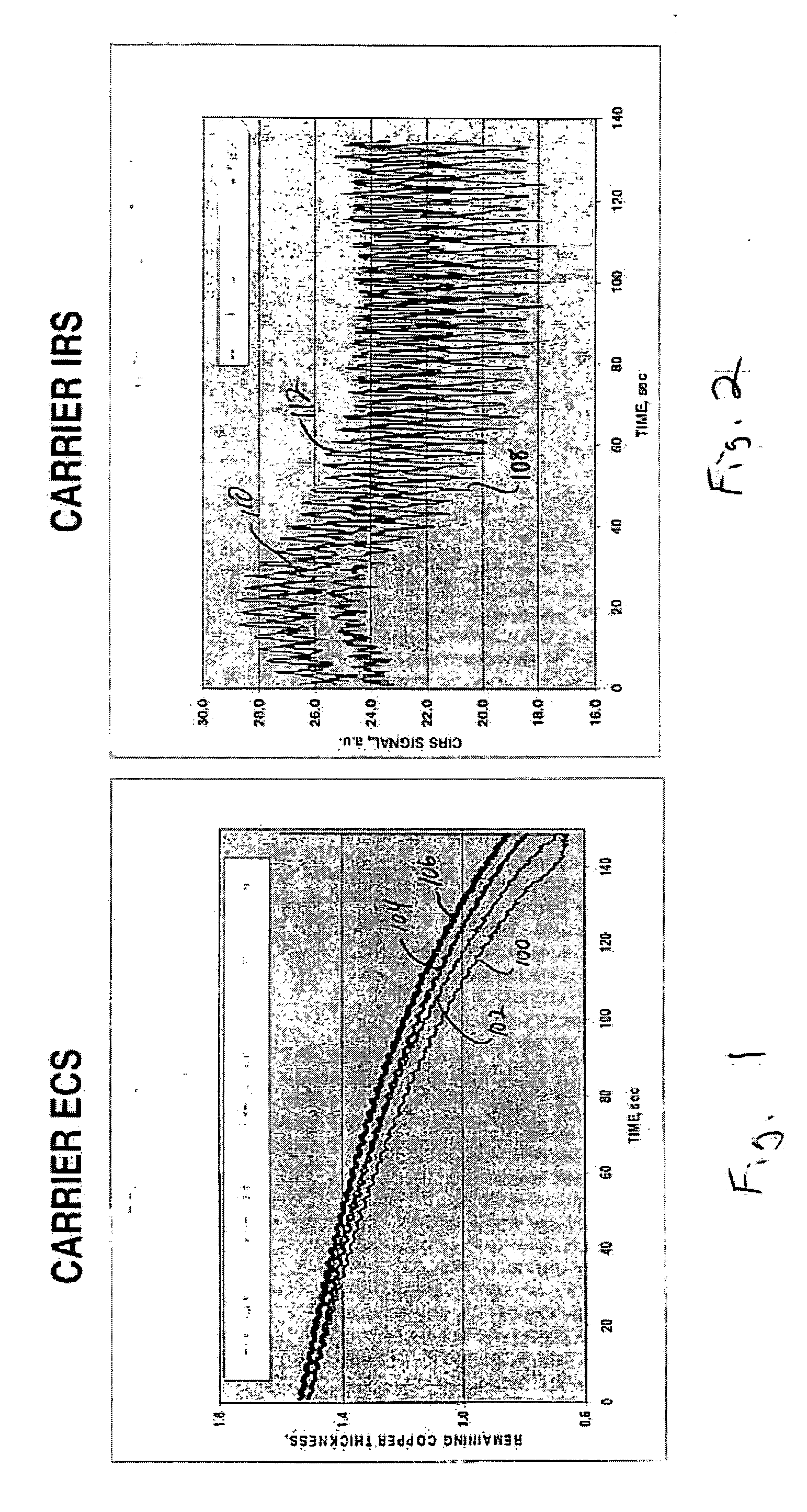
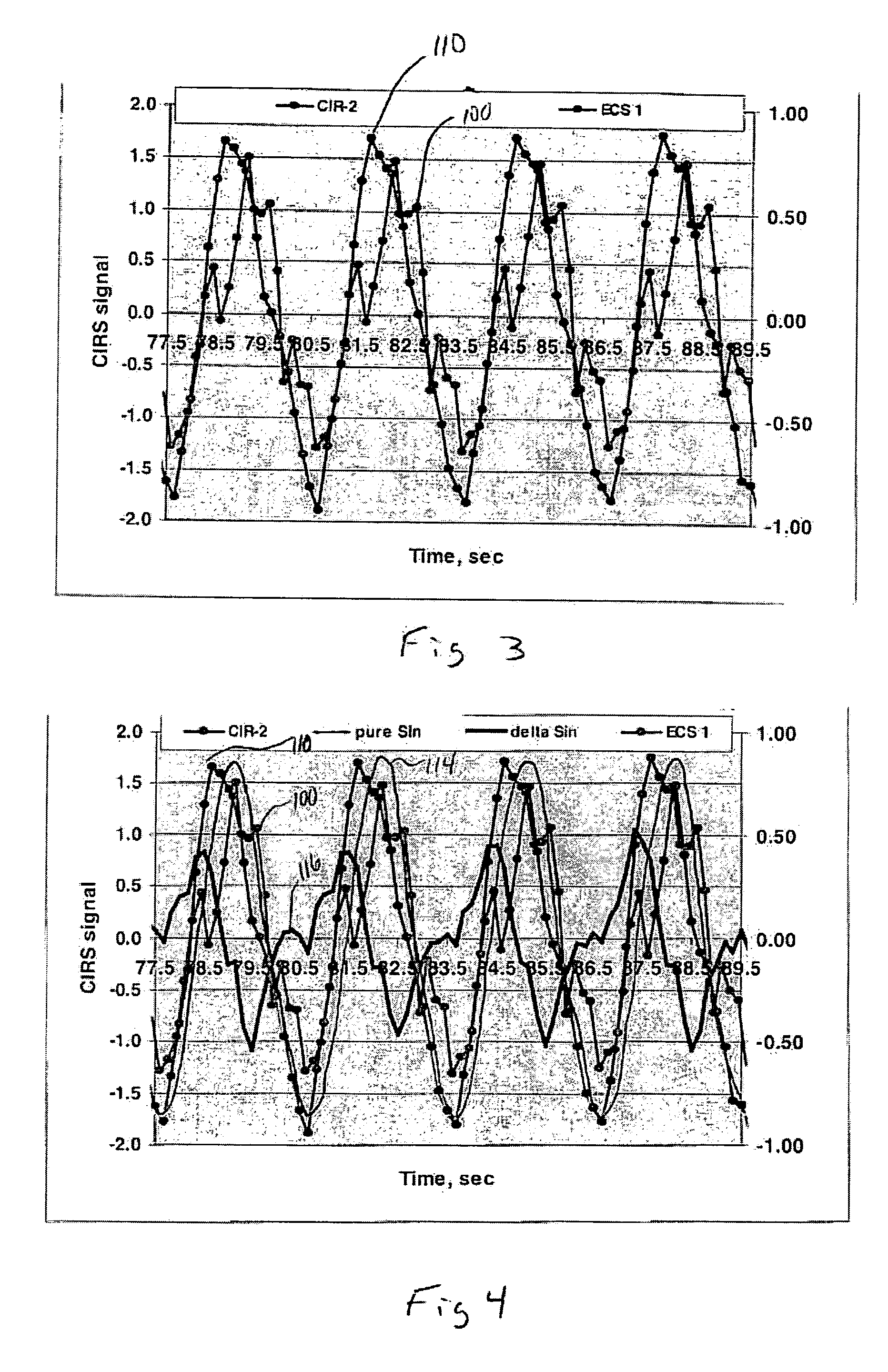
[0028] Eddy current sensors (ECS) allow for measuring a metal film thickness of a moving wafer. The ECS is also capable of functioning as a proximity sensor. Infrared sensors are capable of providing contact-less surface temperature monitoring for a wafer being processed. The embodiments of the present invention provide for real-time contact-less monitoring of stress conditions created through thermal or mechanical conditions....


PUM


Abstract

A chemical mechanical planarization (CMP) system is provided. The CMP system includes a wafer carrier configured to support a wafer during a planarization process, the wafer carrier including a sensor configured to detect a signal indicating a stress being experienced by the wafer during planarization. A computing device in communication with the sensor is included. The computing device is configured to translate the signal to generate a stress map for analysis. A stress relief device responsive to a signal received from the computing device is included. The stress relief device is configured to relieve the stress being experienced by the wafer.

Description

CROSS REFERENCE TO RELATED APPLICATION [0001] This application is related to U.S. patent application Ser. No. 10 / 463,256, entitled “METHOD AND APPARATUS FOR APPLYING DIFFERENTIAL REMOVAL RATES TO A SURFACE OF A SUBSTRATE,” filed on Jun. 18, 2003. This application is incorporated herein by reference in its entirety for all purposes.BACKGROUND OF THE INVENTION [0002] The invention relates generally to semiconductor fabrication and more specifically to in-line metrology for process control during wafer processing. [0003] During semiconductor fabrication, the substrate is exposed to localized stress conditions. With respect to Chemical Mechanical Planarization (CMP) operations, where the planarization is achieved by a topography selective chemical mechanical process that includes revolving steps of mechanical surface activation, localized thermal and mechanical stress regions may occur during the processing. [0004] Monitoring thermal conditions at the wafer / pad interaction interface has...

Claims


Application Information

Patent Timeline
IPC IPC(8): B24B37/04B24B49/14B24B49/16
CPCB24B49/16B24B37/015
Inventor GOTKIS, YEHIELKISTLER, RODNEYOWCZARZ, ALEKSANDERHEMKER, DAVIDBRIGHT, NICOLAS J.
Owner LAM RES CORP
Why Eureka
Try Eureka