Germanium-on-insulator fabrication utilizing wafer bonding

a technology of wafer bonding and germanium on insulator, applied in the field of microelectronic processing, can solve the problems of many obstacles associated with goi fabrication, device scaling continues to decrease, and microelectronic technology will face major roadblocks

Inactive Publication Date: 2005-03-31
INTEL COROIRATION
View PDF6 Cites 46 Cited by
  • Summary
  • Abstract
  • Description
  • Claims
  • Application Information

AI Technical Summary

Problems solved by technology

Microelectronic technology will face major roadblocks in the development of advanced transistors structures as device scaling continues to decrease.
However, there are many obstacles associated with GOI fabrication, especially when using wafers that are 300 mm in scale.
For example, epitaxial growth of germanium directly onto an insulator layer (e.g. silicon dioxide) yields an amorphous germanium layer that is substantially ineffective for microelectronic devices.
In addition, the mismatch between the crystal lattices of the germanium and oxide layers may inhibit direct epitaxial germanium growth on an oxide layer due to unacceptable levels of induced stress.
Furthermore, even though GOI substrates can be fabricated by bonding an oxide substrate such as an oxide wafer, for example, to a germanium wafer, germanium wafers are scarce and expensive.
They are also heavy and fragile compared to silicon wafers.

Method used


Image

  • Germanium-on-insulator fabrication utilizing wafer bonding
  • Germanium-on-insulator fabrication utilizing wafer bonding
  • Germanium-on-insulator fabrication utilizing wafer bonding

Examples


Embodiment Construction

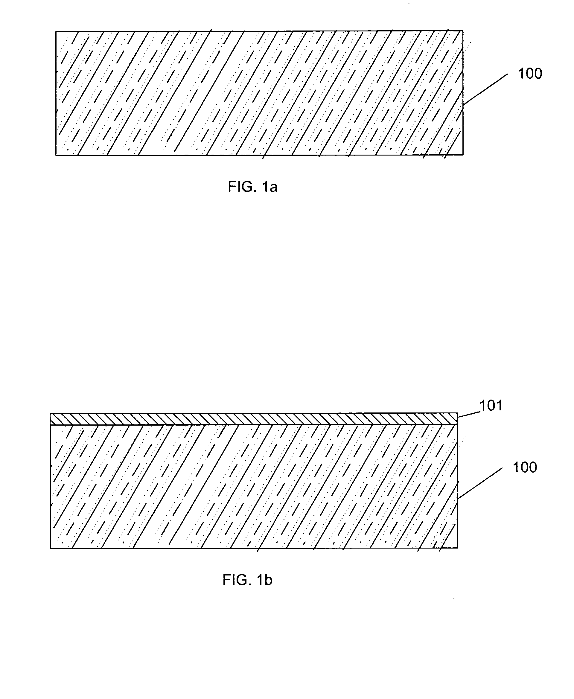
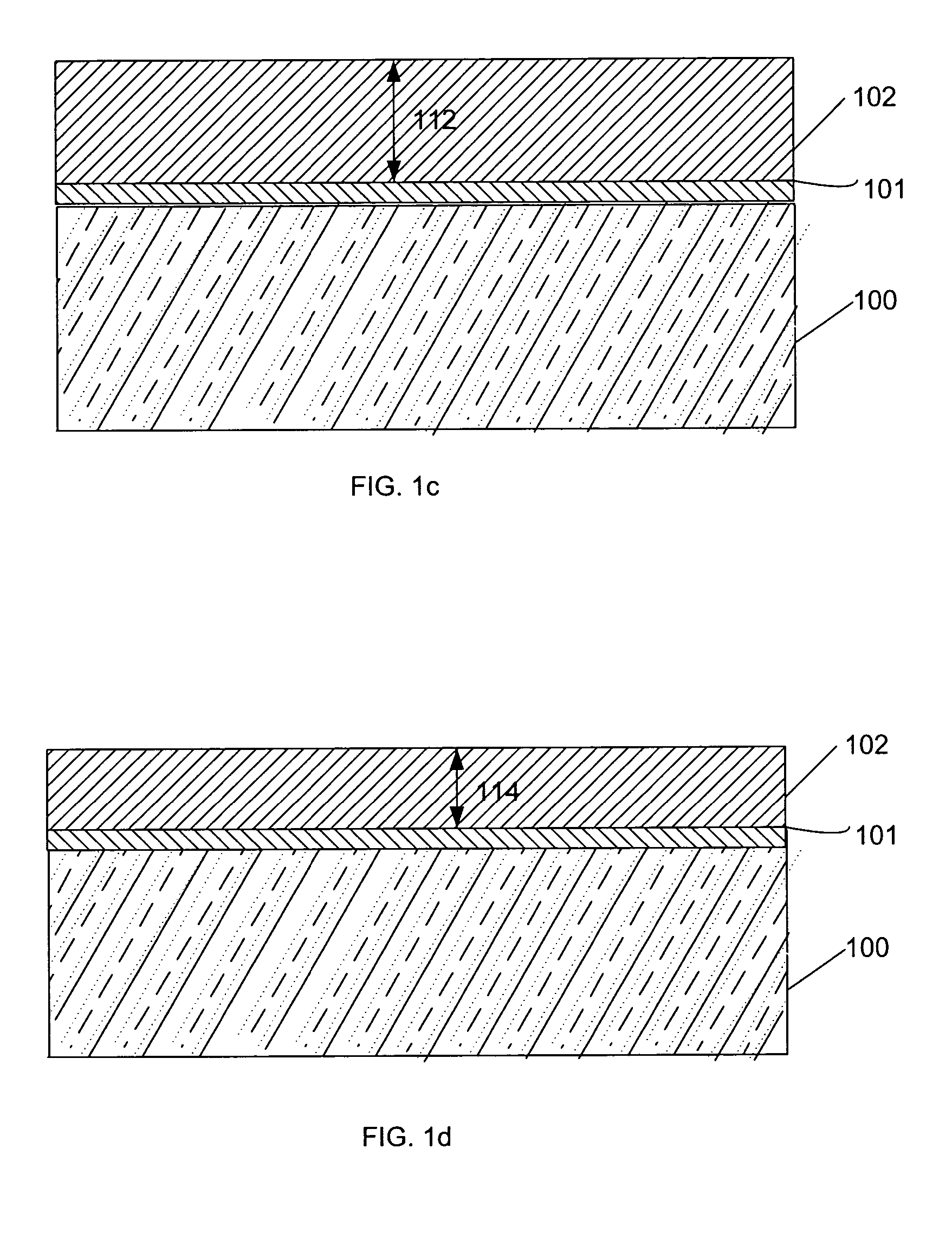
[0008] In the following detailed description, reference is made to the accompanying drawings that show, by way of illustration, specific embodiments in which the invention may be practiced. These embodiments are described in sufficient detail to enable those skilled in the art to practice the invention. It is to be understood that the various embodiments of the invention, although different, are not necessarily mutually exclusive. For example, a particular feature, structure, or characteristic described herein, in connection with one embodiment, may be implemented within other embodiments without departing from the spirit and scope of the invention. In addition, it is to be understood that the location or arrangement of individual elements within each disclosed embodiment may be modified without departing from the spirit and scope of the invention. The following detailed description is, therefore, not to be taken in a limiting sense, and the scope of the present invention is defined...


PUM

PropertyMeasurementUnit
thicknessaaaaaaaaaa
thicknessaaaaaaaaaa
temperatureaaaaaaaaaa

Abstract

Methods of forming a germanium on insulator structure and its associated structures are described. Those methods comprise forming an epitaxial germanium layer on a sacrificial silicon layer, removing a portion of the epitaxial germanium layer, activating the epitaxial germanium layer and an oxide layer disposed on a silicon substrate in an oxygen plasma, and bonding the epitaxial germanium layer to the oxide layer to form a germanium on insulator structure.

Description

FIELD OF THE INVENTION [0001] The present invention relates to the field of microelectronic processing, and more particularly to methods of forming a germanium on insulator structure and structures formed thereby. BACK GROUND OF THE INVENTION [0002] Microelectronic technology will face major roadblocks in the development of advanced transistors structures as device scaling continues to decrease. Building advanced microelectronic devices on germanium substrates has become increasingly more attractive due to the very high mobility of both electrons and holes in the germanium substrate. Germanium substrates can potentially provide improved performance as compared to advanced strained silicon layers, for example. Devices fabricated on germanium on insulator (GOI) substrates (e.g., a substrate that may comprise a germanium layer disposed on an insulator that is disposed on a substrate, such as silicon) are further enhanced due to the leakage reduction potential of the buried insulating l...

Claims


Application Information

Patent Timeline
Patent Type & Authority Applications(United States)
IPC IPC(8): H01L21/762
CPCH01L21/76256
Inventor LEI, RYANSHAHEEN, MOHAMAD
Owner INTEL COROIRATION
Why Eureka
Try Eureka