Self-aligned gated carbon nanotube field emitter structures and associated methods of fabrication

a carbon nanotube and emitter technology, applied in the field of nanotechnology, can solve the problems of limiting the operating life, degrading the performance of the fea, and affecting the operation efficiency of the fea, and achieve the effect of simple, cost-effective and efficien

Inactive Publication Date: 2005-03-31
GENERAL ELECTRIC CO
View PDF7 Cites 27 Cited by
  • Summary
  • Abstract
  • Description
  • Claims
  • Application Information

AI Technical Summary

Benefits of technology

[0007] In various embodiments, the present invention provides a method for fabricating a self-aligned gated (triode) carbon nanotube field emitter structure, including a plurality of sharp, point-like electron emission sources (each consisting of only one or a few carbon nanotubes). The method of the present invention also provides carbon nanotubes that are aligned substantially perpendicular to the associated gate, eliminating the shorting a

Problems solved by technology

The ions bombard the micro-tips, potentially damaging them.
Likewise, the micro-tips are subject to pollution and deterioration, degrading the performance of the FEA and limiting its operating life.
Conventional carbon nanotube FEAs fabricated using a modified Spindt-like process, however, suffer from several problems.
The first problem is that each micro-cavity co

Method used


Image

  • Self-aligned gated carbon nanotube field emitter structures and associated methods of fabrication
  • Self-aligned gated carbon nanotube field emitter structures and associated methods of fabrication
  • Self-aligned gated carbon nanotube field emitter structures and associated methods of fabrication

Examples


Embodiment Construction

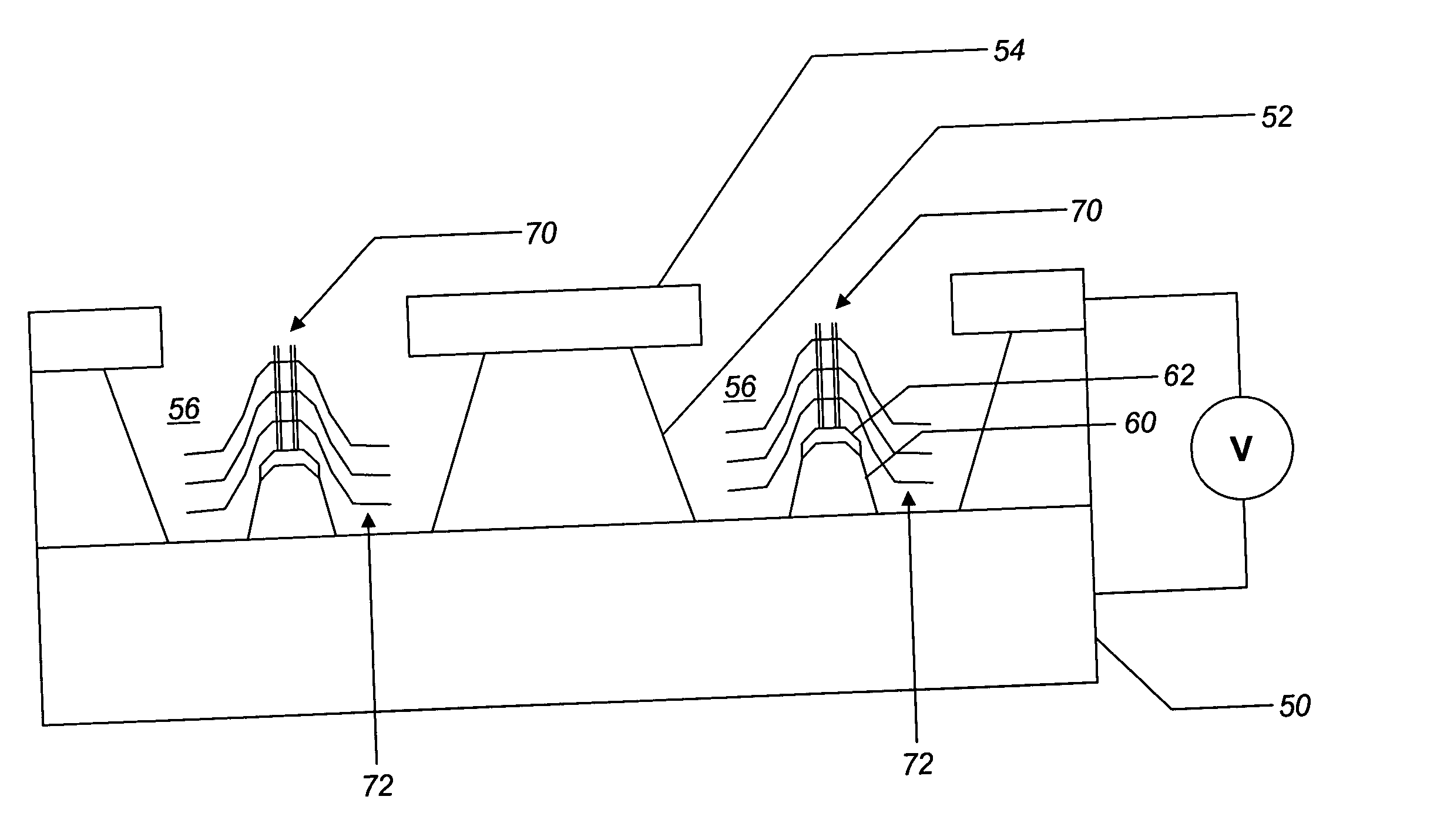
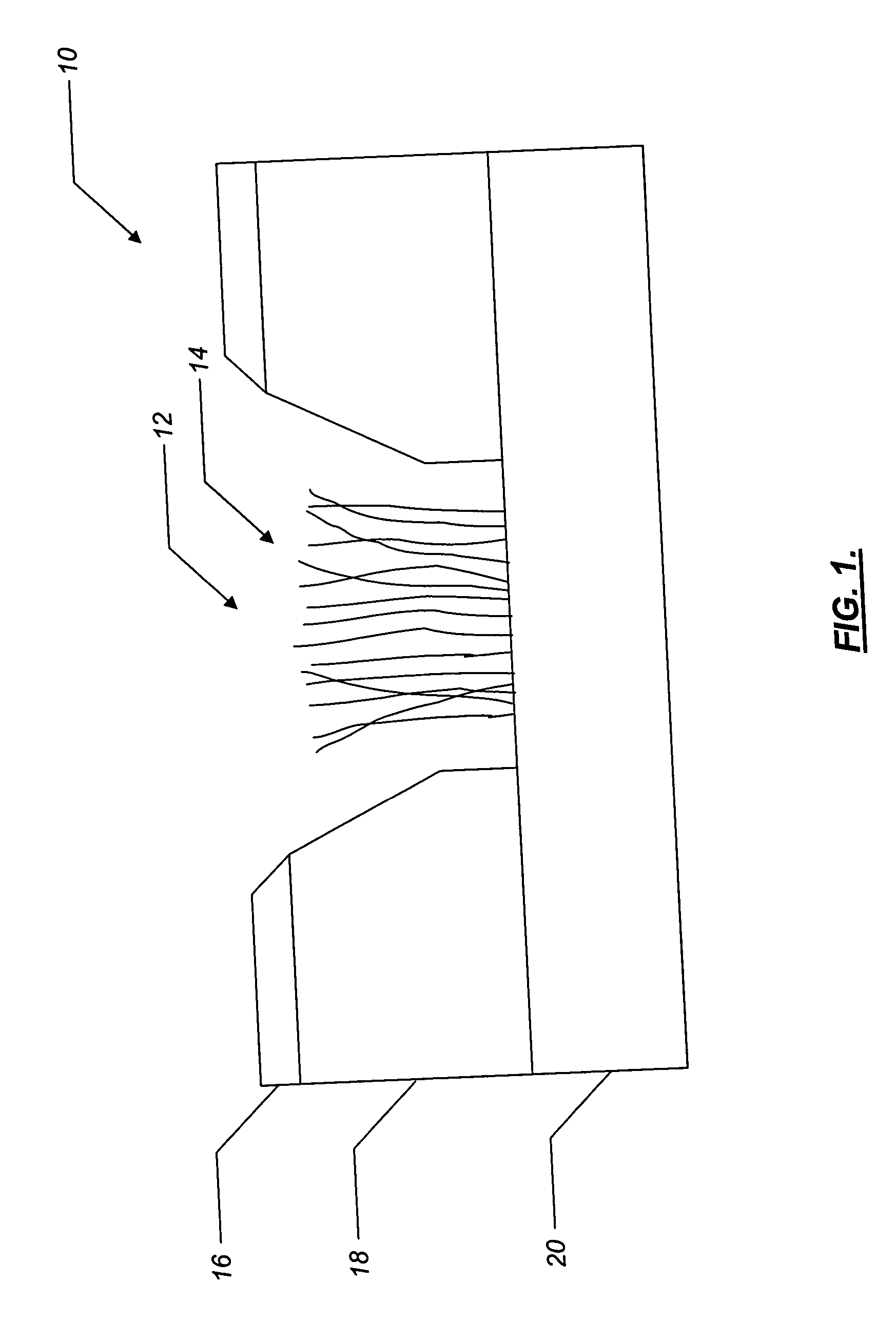
[0019] Referring to FIG. 1, as described above, a conventional carbon nanotube field emitter array (“FEA”) 10 fabricated using a modified Spindt-like process suffers from several problems. The first problem is that each micro-cavity 12 of the carbon nanotube FEA 10 contains a tangled mass of carbon nanotubes 14. This tangled mass of carbon nanotubes 14 behaves as a block conductor. Preferably, a field emitter structure includes a plurality of sharp, point-like electron emission sources (each consisting of only one or a few carbon nanotubes), rather than a block conductor. The second problem is that the carbon nanotubes are generally, but not universally, aligned perpendicular to the associated anode or gate electrode 16 (a dielectric layer 18 and a cathode electrode 20 are also illustrated). Under electrostatic forces, the off-angle carbon nanotubes may be displaced and short to the gate. Likewise, the off-angle carbon nanotubes may result in emission into the gate. Preferably, all ...


PUM


Abstract

A method for fabricating a self-aligned gated carbon nanotube field emitter structure includes providing a substrate, depositing a dielectric material on the surface of the substrate and depositing a conductor layer on the surface of the dielectric material. The method also includes selectively etching the conductor layer to form an opening and selectively etching the dielectric material to form a micro-cavity. The method further includes depositing a base layer structure in the micro-cavity adjacent to the surface of the substrate, wherein the base layer structure has a substantially conical shape, and depositing a catalyst on a portion of the surface of the base layer structure, wherein the catalyst is suitable for growing at least one carbon nanotube. The method still further includes applying an electrical potential to the substrate and the conductor layer, wherein the electrical potential generates a plurality of electrical field lines that are deflected around the surface of the base layer structure, and wherein the plurality of electrical field lines have a strength that is greatest in a direction substantially perpendicular to the surface of the substrate. Finally, the method includes growing at least one carbon nanotube from the catalyst in the presence of the plurality of electrical field lines, wherein the at least one carbon nanotube is grown in a direction substantially perpendicular to the surface of the substrate.

Description

FIELD OF THE INVENTION [0001] The present invention relates generally to the field of nanotechnology. More specifically, the present invention relates to self-aligned gated carbon nanotube field emitter structures and associated methods of fabrication. BACKGROUND OF THE INVENTION [0002] Carbon nanotubes are currently being considered as electron emission sources in, for example, flat panel field emission display (“FED”) applications, microwave power amplifier applications, transistor applications and electron-beam lithography applications. The carbon nanotubes are typically configured in a triode field emitter structure, including a plurality of carbon nanotubes disposed within a plurality of micro-cavities that are arranged in an array, a common anode or gate electrode for modulating an emission (tunneling) current, a common dielectric layer and a common cathode electrode. The carbon nanotubes are typically disposed within the plurality of micro-cavities through an arc discharge me...

Claims


Application Information

Patent Timeline
IPC IPC(8): H01J3/02H01J9/02
CPCB82Y10/00H01J2201/30469H01J9/025H01J3/022
Inventor LEE, JI UNGHUBER, WILLIAM HULLINGER
Owner GENERAL ELECTRIC CO
Why Eureka
Try Eureka