
Variable inductor for integrated circuit and printed circuit board

a technology of printed circuit board and inductor, which is applied in the field of circuits, can solve the problems of reducing the performance of the inductor, resulting in higher cost, and achieve the effect of convenient fabrication and good rf performan

Inactive Publication Date: 2005-03-31
QUALCOMM INC
View PDF9 Cites 111 Cited by
  • Summary
  • Abstract
  • Description
  • Claims
  • Application Information

AI Technical Summary

Benefits of technology

A variable inductor that can be conveniently fabricated on an integrated circuit or a printed circuit board is described herein. The variable inductor has good RF performance and may be used for various applications such as filters, VCOs, impedance matching networks, and so on.

Problems solved by technology

However, the bank of inductors occupies a large area, which translates into higher cost.
Moreover, the series-coupled switch can degrade the performance of the inductor.

Method used


Image

  • Variable inductor for integrated circuit and printed circuit board
  • Variable inductor for integrated circuit and printed circuit board
  • Variable inductor for integrated circuit and printed circuit board

Examples


Embodiment Construction

The word “exemplary” is used herein to mean “serving as an example, instance, or illustration.” Any embodiment or design described herein as “exemplary” is not necessarily to be construed as preferred or advantageous over other embodiments or designs.

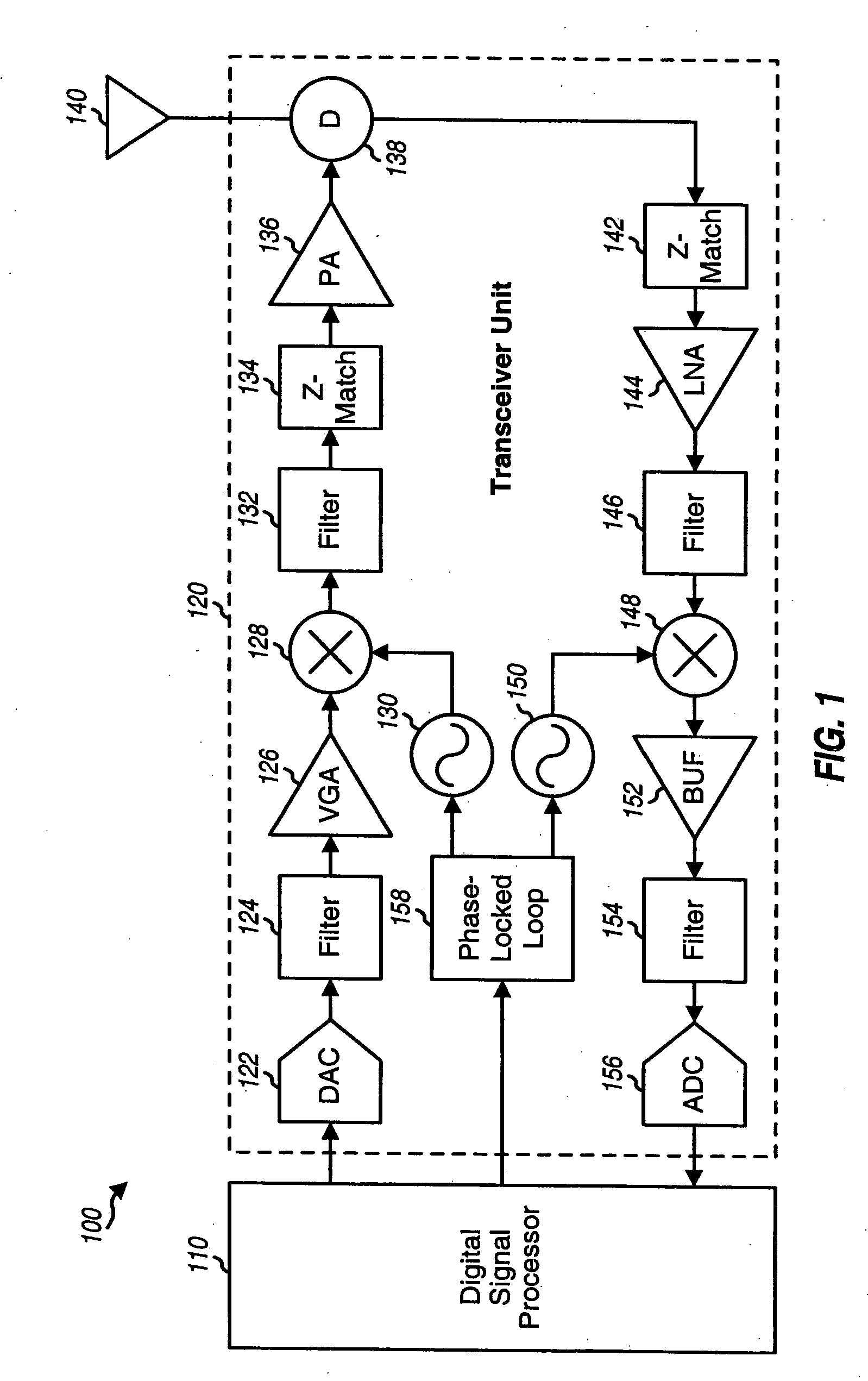
FIG. 1 shows a block diagram of a wireless terminal 100 that may be used for wireless communication. On the transmit path, a digital signal processor (DSP) 110 processes data to be transmitted and provides a stream of chips to a transceiver unit 120. Within transceiver unit 120, one or more digital-to-analog converters (DACs) 122 convert the stream of chips to one or more analog signals. The analog signal(s) are filtered by a filter 124, amplified by a variable gain amplifier (VGA) 126, and frequency upconverted from baseband to radio frequency (RF) by a mixer 128 to generate an RF signal. The frequency upconversion is performed with an upconversion local oscillator (LO) signal from a VCO 130. The RF signal is filtered by a filter 132...


PUM

PropertyMeasurementUnit
inductanceaaaaaaaaaa
impedanceaaaaaaaaaa
frequenciesaaaaaaaaaa

Abstract

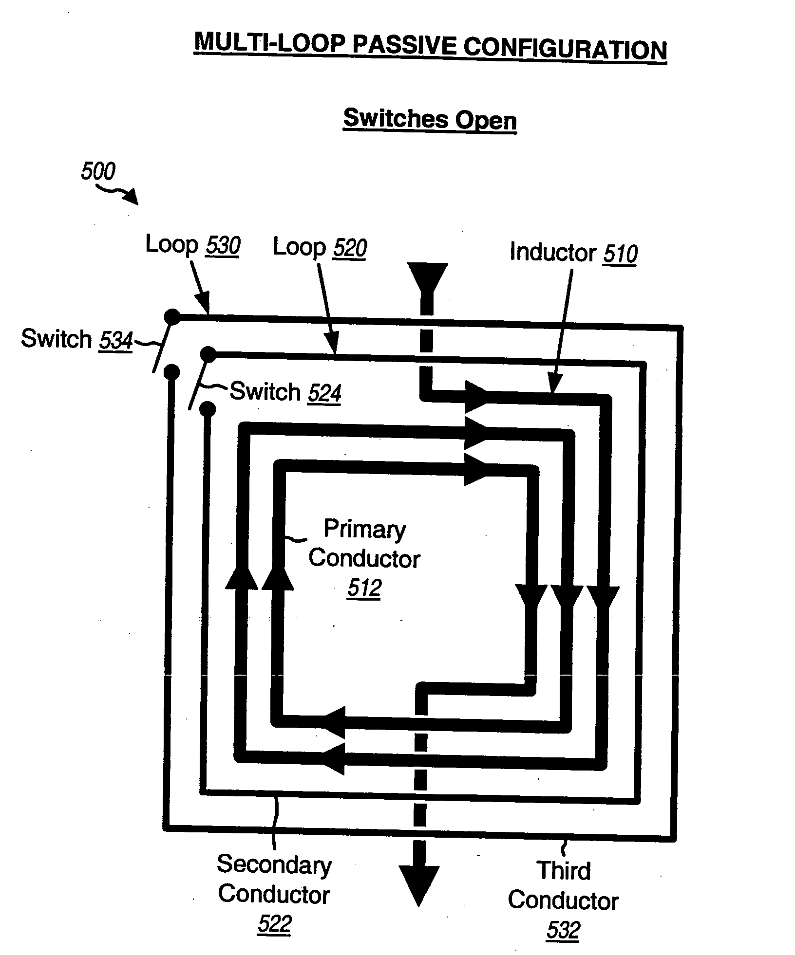
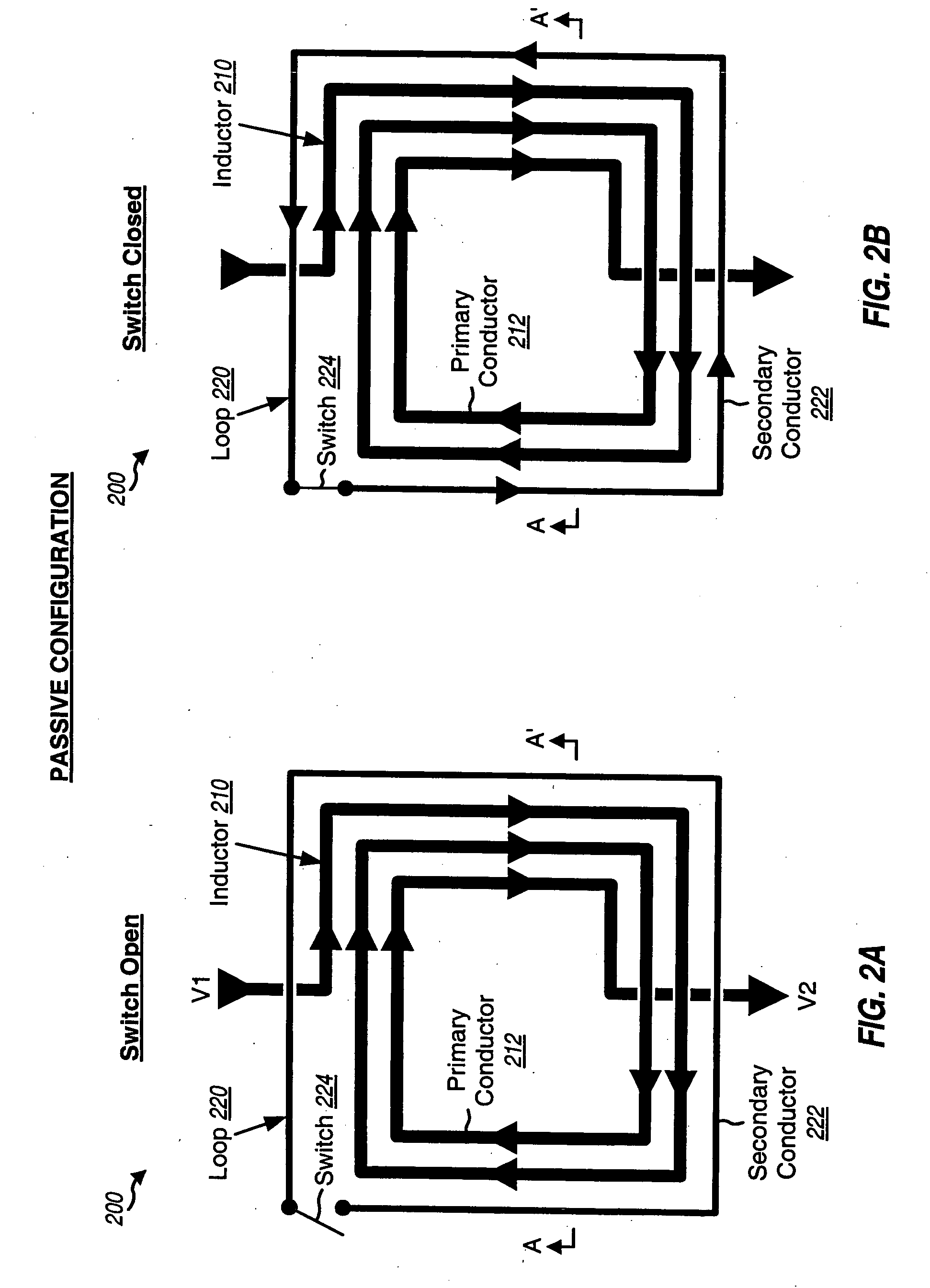
A variable inductor can be formed on an integrated circuit with a primary conductor, a secondary conductor, and a switch. The primary conductor implements an inductor and may be formed in various patterns (e.g., a spiral). The secondary conductor forms a loop in proximity to (e.g., on the outside of) the primary conductor. The switch couples in series with the secondary conductor and opens or closes the loop. The inductance of the inductor is varied by closing and opening the loop with the switch. A current source may also be coupled in series with the secondary conductor and used to control the current flow in the secondary conductor to either increase or decrease the inductance. Multiple loops may be formed to change the inductance in more than two discrete steps. The variable inductor may be used for various applications such as filters, VCOs, and impedance matching networks.

Description

BACKGROUND I. Field The present invention relates generally to circuits, and more specifically to an inductor for an integrated circuit and a printed circuit board. II. Background With modern advances in integrated circuit (IC) process technology, it is possible to fabricate radio frequency integrated circuits (RFICs) for numerous applications such as wireless communication, networking, computing, and so on. These RFICs may include various analog circuit blocks that were previously implemented with bulky discrete circuit components. By implementing analog circuit blocks on RFICs, various benefits such as smaller size, lower cost, and improved reliability can be realized. Many analog circuit blocks utilize reactive components such as capacitors and inductors to achieve the designed functions. For example, filters, resonator tanks, impedance matching networks, and so on may include both capacitors and inductors to obtain the desired circuit response. For some applications, such a...

Claims


Application Information

Patent Timeline
Patent Type & Authority Applications(United States)
IPC IPC(8): H01F17/00H01F21/12H01L23/522H01L27/08
CPCH01F17/0006H01F21/12H01F2021/125H01L23/5227H01L27/08H01L2924/0002H01L2924/3011H03J2200/35H01L2924/00H01L27/04
Inventor JESSIE, DARRYL
Owner QUALCOMM INC
Learn More